Method for preparing micro-nano structure on the surface of tungsten material and tungsten material with micro-nano structure on the surface and application thereof

A micro-nano structure and nano-technology, applied in the field of material surface micro-nano structure preparation, can solve the problems of large reaction area, low precision, and low preparation efficiency

Active Publication Date: 2021-05-04
INST OF ELECTRICAL ENG CHINESE ACAD OF SCI
View PDF5 Cites 0 Cited by
  • Summary
  • Abstract
  • Description
  • Claims
  • Application Information

AI Technical Summary

Problems solved by technology

However, the processing efficiency of grinding and polishing methods is very low; electrolytic polishing cannot achieve ultra-smooth surface quality; plasma polishing cannot guarantee the same roughness of each point on the surface of the material due to the large reaction area; Electrolysis, the micro-nano structure of the surface cannot be quantitatively controlled; plasma polishing also etches the surface of the entire material, and the micro-nano structure of the surface cannot be quantitatively controlled either
Therefore, the above-mentioned polishing method is limited by its technology, and has defects such as low preparation efficiency, low precision, and incapable of quantitative control.

Method used


Image

  • Method for preparing micro-nano structure on the surface of tungsten material and tungsten material with micro-nano structure on the surface and application thereof
  • Method for preparing micro-nano structure on the surface of tungsten material and tungsten material with micro-nano structure on the surface and application thereof
  • Method for preparing micro-nano structure on the surface of tungsten material and tungsten material with micro-nano structure on the surface and application thereof

Examples


preparation example Construction

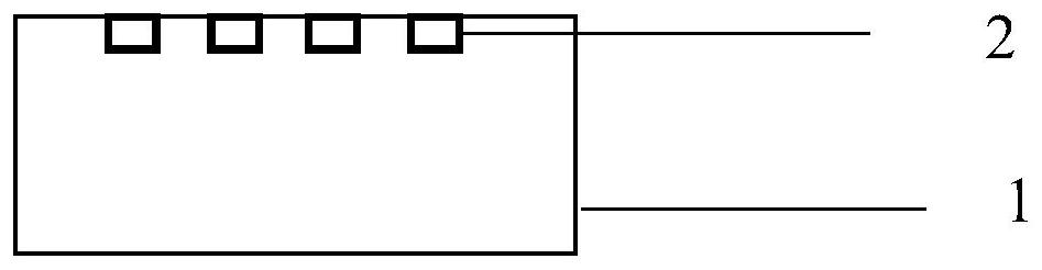
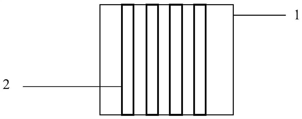
[0023] The invention provides a method for preparing a micro-nano structure on the surface of a tungsten material, comprising the following steps:

[0024] Under vacuum conditions, use a helium ion microscope to perform the first ion etching on the surface of the tungsten material to obtain etched micro-regions;

[0025] Under vacuum conditions, the second ion etching is performed on the etched micro-region by using a helium ion microscope, forming nano-stripes in the etched micro-region, and obtaining a micro-nano structure on the surface of the tungsten material.

[0026] In the invention, the first ion etching is carried out on the surface of the tungsten sheet by using a helium ion microscope under vacuum conditions to obtain etched micro-regions.

[0027] In the present invention, the tungsten material preferably includes sequential machining, polishing and ultrasonic cleaning before use. In the present invention, there is no special limitation on the mechanical processi...

Embodiment 1

[0039] The tungsten block is prepared by mechanical processing into a tungsten sheet with a diameter of 3 mm and a thickness of 1 mm, and then mechanically polished to a surface roughness of 2 μm, and then ultrasonically cleaned with industrial ethanol at 300 W for 5 minutes to obtain a tungsten material;

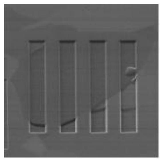
[0040] The tungsten material is placed in a helium ion microscope, and the vacuum degree is pumped to 10 -3 When Pa is lower than Pa, the gallium ion source is used to perform the first ion etching on any surface of the tungsten sheet to obtain a square etched micro-region with a side length of 5 μm and an etching depth of 5 μm. The working conditions of the helium ion microscope are: accelerated The voltage is 25kV, the beam current is 10pA, and the incident angle is 45°;

[0041] The resulting tungsten material with etched micro-regions was placed in a helium ion microscope at a vacuum of 10 -3 Under the condition below Pa, the gallium ion source is used to carry out the...

Embodiment 2

[0043] The tungsten block is prepared by mechanical processing into a tungsten sheet with a diameter of 10mm and a thickness of 2mm. After mechanical polishing, the surface roughness is 5μm, and then ultrasonic cleaning is performed with industrial ethanol at 700W for 10min to obtain a tungsten material;

[0044] The tungsten material is placed in a helium ion microscope, and the vacuum degree is pumped to 10 -3 When Pa is lower than Pa, the gallium ion source is used to perform the first ion etching on any surface of the tungsten sheet to obtain a square etched micro-region with a side length of 10 μm and an etching depth of 5 μm. The working conditions of the helium ion microscope are: accelerated The voltage is 30kV, the beam current is 15pA, and the incident angle is 45°;

[0045] The resulting tungsten material with etched micro-regions was placed in a helium ion microscope at a vacuum of 10 -3 Under the condition below Pa, the gallium ion source is used to carry out the...


PUM

PropertyMeasurementUnit
lengthaaaaaaaaaa
depthaaaaaaaaaa
lengthaaaaaaaaaa

Abstract

The invention provides a method for preparing a micro-nano structure on the surface of a tungsten material, a tungsten material with a micro-nano structure on the surface and an application thereof, belonging to the technical field of material surface microstructure. The method for preparing a micro-nano structure on the surface of a tungsten material provided by the present invention comprises the following steps: under vacuum conditions, using a helium ion microscope to perform the first ion etching on the surface of the tungsten material to obtain etched micro-regions; and performing second ion etching on the etched micro-region by using a helium ion microscope, forming nano-stripes in the etched micro-region, and obtaining a micro-nano structure on the surface of the tungsten material. The preparation method provided by the invention operates under vacuum conditions and is not easily polluted; the helium ion microscope has ultra-high-precision multifunctional processing capabilities, and the micro-nano structure prepared by the helium ion microscope is highly accurate; it can realize the micro-nano structure. Quantitative control; and simple process and low cost.

Description

technical field [0001] The invention relates to the technical field of preparation of micro-nano structures on the surface of materials, in particular to a method for preparing micro-nano structures on the surface of tungsten materials, tungsten materials with micro-nano structures on the surface and applications thereof. Background technique [0002] Tungsten has been recognized as the most promising plasma-facing material for tokamak devices due to its high melting point, good thermal conductivity, and low sputtering yield. However, the interaction between tungsten and fusion reaction product helium will cause radiation damage such as blistering and embrittlement of tungsten materials, which will seriously affect the service life of tungsten materials and the stability of fusion reactions. [0003] In order to solve the foaming problem of tungsten materials, the number of material surface interfaces can be increased by changing the surface roughness of the material, and th...

Claims


Application Information

Patent Timeline
Patent Type & Authority Patents(China)
IPC IPC(8): C23F4/00G21B1/05B82Y40/00
CPCB82Y40/00C23F4/00G21B1/057Y02E30/10
Inventor 马玉田刘俊标韩立
Owner INST OF ELECTRICAL ENG CHINESE ACAD OF SCI
Why Eureka
Try Eureka