Process for manufacturing a resin-encapsulated electronic product

a technology of electronic products and resins, applied in the field of resin-encapsulated electronic products, can solve the problems of reducing the yield of such resin-encapsulated electronic products, and achieve the effect of preventing the decline in the yield

Inactive Publication Date: 2000-04-25
PANASONIC CORP
View PDF15 Cites 9 Cited by
  • Summary
  • Abstract
  • Description
  • Claims
  • Application Information

AI Technical Summary

Benefits of technology

An object of the present invention is to provide a manufacturing method of small electronic components, by which a decline in the yield is prevented.
According to the manufacturing method of the present invention, in the package layer forming step, the electronic component, the printed circuit substrate, and the solder paste are all protected by the coating layer which has a distinct heat-resisting property and are thereby prevented from being directly contacted with the melted thermoplastic resin. Accordingly, the electronic components are prevented from being damaged by heat, since the heat stress exerted thereto is alleviated due to the coating layer which blocks the heat conductance from the thermoplastic resin. Also, the shearing strain which is exerted on the electronic components and the solder paste from the inflow of the thermoplastic resin is remarkably reduced as compared with the case in which they are not covered with the coating layer because they are fixed by the coating layer. Thus, it is avoided that the electronic components are displaced or a part of the solder paste melts and flows away. Accordingly, highly favorable sealing in terms of functions and reliability can be achieved with the package layer of the thermoplastic resin, and the yield of the finished resin-encapsulated electronic product is remarkably enhanced.
Since silicon has a high heat-resisting property, it can certainly protect the electronic components and the substrate from the heat from the thermoplastic resin which has been melted at a high temperature in the package layer forming step. Further, silicon has also a favorable electric insulating function because of its excellent dielectric characteristic, anti-partial discharge characteristic, and arc resisting characteristic. On the other hand, crystal polymer has a high molding characteristic, by which a favorable package layer can be formed.

Problems solved by technology

However, the above-described conventional manufacturing method has such a drawback that when the thermoplastic resin 12 is injected into the cavity 10 from the orifice 11, the heated and melted resin 12 tends to cause various defects: for example the electronic components 2-4 may be damaged by heat; a part of solder paste which connects the electronic components 2-4 on the substrate 1 may melt and flow away; or electronic components may be shoved and thus displaced from a certain mounting position.
There has been a problem of decrease in the yield of such resin-encapsulated electronic products 13 due to these defects.

Method used


Image

  • Process for manufacturing a resin-encapsulated electronic product
  • Process for manufacturing a resin-encapsulated electronic product
  • Process for manufacturing a resin-encapsulated electronic product

Examples


Embodiment Construction

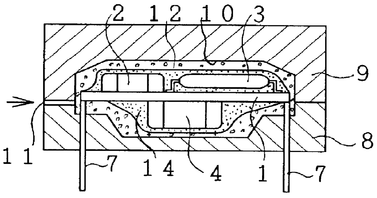
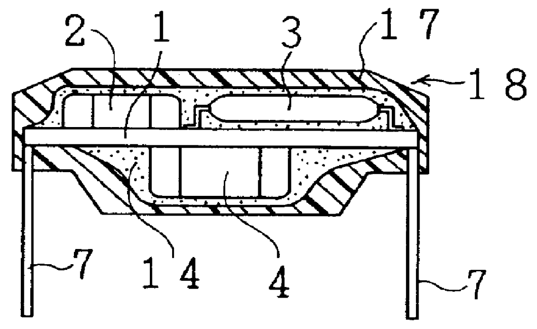
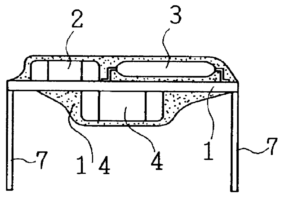
Preferred embodiments of the present invention will be hereinafter described referring to the drawings. FIGS. 1A-1D show a manufacturing method according to one embodiment of the present invention in order of processing steps.

First, as shown in FIG. 1A, a double-side printed circuit substrate 1, on both sides of which predetermined printed patterns are formed, is mounted with necessary electronic components 2-4 by soldering, and connected with lead elements 7 at its both ends, so as to be assembled to have certain required functions, for example, as a gas meter or other appliances.

Next, as shown in FIG. 1B, the printed circuit substrate 1 including the electronic components 2-4 in its entirety is covered with a coating layer 14 to be hermetically sealed. For forming the coating layer 14, a silicone having high thermal resistance (for example, Article No. AX42-360, Dow Corning Toray Silicone Co., Ltd.) is used as a coating material, with which the whole printed circuit substrate 1 in...


PUM

PropertyMeasurementUnit
mold temperatureaaaaaaaaaa
heat resistanceaaaaaaaaaa

Abstract

PCT No. PCT / JP96 / 03578 Sec. 371 Date Jun. 3, 1998 Sec. 102(e) Date Jun. 3, 1998 PCT Filed Dec. 6, 1996 PCT Pub. No. WO97 / 20673 PCT Pub. Date Jun. 12, 1997The present invention provides a method of manufacturing a small electronic component, by which its yield can be enhanced. The invention comprises the steps of: a component mounting step of mounting a necessary electronic component 2-4 on a substrate 1; a coating layer forming step of forming a coating layer 14 for covering and sealing the substrate 1 in its entirety including the electronic component 2-4 with a coating material having high heat resistance; and a package layer forming step of forming a package layer 17 for covering and sealing a circumference of the coating layer 14 with a thermoplastic resin material 12. In the package layer forming step, adverse effects by the heat from the thermoplastic resin 12 to the electronic components 2-4 and the substrate 1 are inhibited with the coating layer 14.

Description

The present invention relates to a method for manufacturing a resin-encapsulated electronic product which consists of a substrate on which required electronic components are mounted and are entirely sealed in a resin for packaging.A resin-encapsulated electronic product is generally manufactured through such processes as described below. Specifically, as shown in FIG. 2A, the product is assembled such that a double-side printed circuit substrate 1, on both sides of which predetermined printed patterns are formed, is mounted with necessary electronic components 2-4 by soldering and is connected with lead elements 7 at its both ends, so as to have certain required functions, for example, as a gas meter or other appliances. Next, as shown in FIG. 2B, the entire printed circuit substrate 1 including the electronic components 2-4 is inserted into a cavity 10 formed by a lower mold 8 and an upper mold 9, after which both molds 8, 9 are clamped together. Successively, a thermoplastic resin...

Claims


Application Information

Patent Timeline
Patent Type & Authority Patents(United States)
IPC IPC(8): B29C45/14B29C70/00B29C70/68H01L21/02H01L21/56H01L23/28H01L23/31H05K3/28B29L31/34C08L83/00C08L83/02C09D201/00H01L23/29
CPCB29C45/14639B29C45/14655B29C45/14836B29C70/683H01L21/565H01L23/3135H05K3/284Y10T29/49002H01L2924/0002Y10T29/4913Y10T29/49146Y10T29/49004H01L2924/00
Inventor YOSHIDA, KOICHIFUKUSHIMA, TETSUOSUETSUGU, KENICHIRO
Owner PANASONIC CORP
Why Eureka
Try Eureka