Electro-absorption type semiconductor optical modulator having a quantum well structure

Inactive Publication Date: 2000-08-08
RENESAS ELECTRONICS CORP
View PDF5 Cites 25 Cited by
  • Summary
  • Abstract
  • Description
  • Claims
  • Application Information

AI Technical Summary

Problems solved by technology

Therefore, the larger the QCSE shift provided by a structure, the larger the amount of QCSE shift caused by its built-in electric field.
Since the QCSE shift caused by the built-in field does not

Method used


Image

  • Electro-absorption type semiconductor optical modulator having a quantum well structure
  • Electro-absorption type semiconductor optical modulator having a quantum well structure
  • Electro-absorption type semiconductor optical modulator having a quantum well structure

Examples


second example

A second example of the present invention is described with reference to FIGS. 6, 7 and 8.

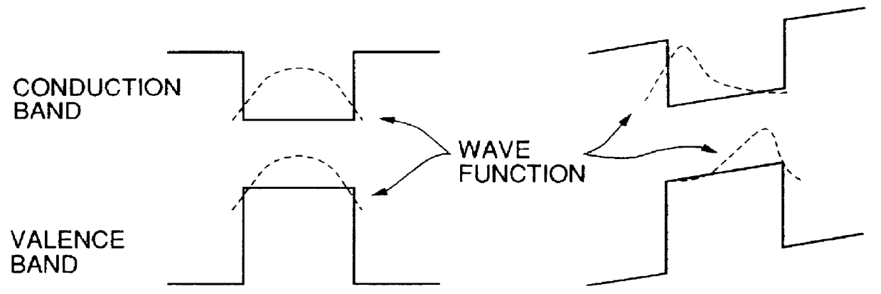
FIG. 7(a) to FIG. 7(d) show cross sectional views of a device during its fabrication process for illustrating the second example. FIG. 8 is a band diagram of the MQW absorption layer. FIG. 6 represents a perspective view of the MQW-EA modulator fabricated by the second example.

It is an example for a different MQW optical absorption layer although the device fabricating process is same as the first example. The MQW optical absorption layer consisted of, as shown in FIG. 8, non-doped In..sub.760 Ga..sub.240 As..sub.511 P..sub.489 (no strain, bandgap wavelength (.lambda.g=1.20 .mu.m thicknessof 15 nm) as an n region side light confinement layer (SCH layer), non-doped In..sub.760 Ga..sub.240 As..sub.511 P..sub.489 (6 nm thick) as a barrier layer, and a well layer. Each one of the single quantum well layers comprised three sequentially layers of a 4 nm thick In..sub.380 Ga..sub.620 As (stain: .epsil...


PUM


Abstract

Disclosed is an electro-absorption type semiconductor optical modulator utilizing the Quantum Confinement Stark Effect, in which a quantum well structure introduced in its optical absorption layer is arranged to have a potential structure such that one of the electron affinity and the energy of the top of the valence band increases in the laminating direction, while the other decreases, thereby canceling the built-in field. It is intended to lower the drive voltage and to enhance an on/off ratio (extinction ratio). Thus, the absorption peak becomes narrow at a no bias state to attain a low drive voltage and an enhanced extinction ratio.

Description

The present invention relates to a semiconductor optical modulator, and more specifically, to a quantum well structured electro-absorption type optical modulator utilizing the Quantum Confinement Stark Effect.DESCRIPTION OF THE RELATED ARTExternal modulation using an electro-absorption (EA) light modulator is a very effective means for long distance fiber optic communication over several tens to several hundreds of kilometers or more at a high speed of 2.5-10 gigabit per second (Gb / s) or higher, because compared with a direct laser modulation system, it has very low wavelength fluctuation (wavelength chirping) when modulated. As shown in FIG. 1, the conventional EA modulator performs the on-off operation by utilizing the fact that, when the modulator is reversely biased, the absorption spectrum shifts to a longer wavelength to vary the absorption coefficient in the operating wavelength. Thus, it is important to obtain larger variation of the absorption coefficient with a low applied...

Claims


Application Information

Patent Timeline
IPC IPC(8): G02F1/017G02F1/01G02F1/015G02F1/025
CPCB82Y20/00G02F1/01725G02F1/01708G02F2001/0157G02F2001/0175G02F2001/01766G02F1/0175G02F1/0157G02F1/01766
Inventor SAKATA, YASUTAKA
Owner RENESAS ELECTRONICS CORP
Why Eureka
Try Eureka