Method for making a silicon single crystal wafer

a single crystal wafer and silicon technology, applied in the direction of polycrystalline material growth, crystal growth process, polycrystalline material growth, etc., can solve the problem of pn junction leakage unfavorable failure, gradient distribution in a radial direction and pulling rate extremely restricted conditions, and inducing osf as a secondary d

Inactive Publication Date: 2000-09-05
SUMITOMO MITSUBISHI SILICON CORP
View PDF5 Cites 15 Cited by
  • Summary
  • Abstract
  • Description
  • Claims
  • Application Information

AI Technical Summary

Benefits of technology

The present invention has been made in view of the problems on methods of manufacturing a silicon single crystal according to the above-stated conventional Czochralski method, and has for its object the provision of a method for manufacturing a silicon single crystal wafer wherein the occurrence of OSF can be suppressed within a zone of latently generating an OSF ring within a wafer and the formation of dislocation clusters within the outside zone of the OSF ring can also be suppressed. In addition, such a manufacturing method has a wide process window, and its productivity is high.

Problems solved by technology

Moreover, when the pulling rate is made smaller than about 0.4 mm / minute, there arises the problem due to the dislocation cluster occurring in the outside zone of the OSF ring.
More particularly, it is not taken into account that dislocation clusters break out in the outside zone of the OSF ring under such manufacturing conditions as mentioned above, and any measure or procedure of preventing the occurrence of the dislocation cluster is not disclosed at all.
Accordingly, it will be apparent that although the GOI characteristic is good in the outside zone of the OSF ring, such a characteristic failure as of pn junction leakage unfavorably takes place owing to the occurrence of the dislocation cluster.
However, this method requires both temperature gradient distributions in a radial direction and pulling rate to be extremely restricted conditions.
This is because an oxygen precipitation nucleus existing in the OSF ring occurring zone in the crystal grows by the high temperature thermal treatment, thereby inducing OSF as a secondary defect.
Such OSF is one of factors of degrading various device characteristics, thereby lowering the device yield.

Method used


Image

  • Method for making a silicon single crystal wafer
  • Method for making a silicon single crystal wafer
  • Method for making a silicon single crystal wafer

Examples


example 1

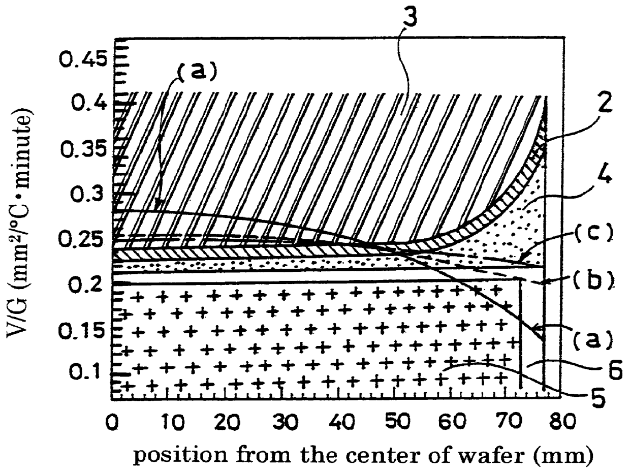
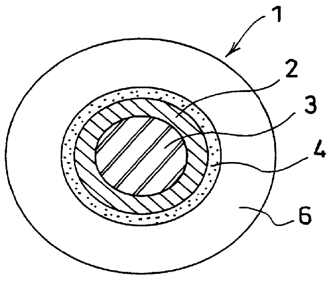
Using a manufacturing apparatus for carrying out the Czochralski method which had a 18" .PHI. quartz crucible and a carbon crucible set therein and which was capable of growing a 6" .PHI. single crystal, a single crystal was pulled. The conditions including a relative position between a cylindrical carbon heater set around the crucible and the crucible, the distance between the tip of an irradiation shielding body of a semi-conical form, which was set about the crucible, was made of carbon, and had a thickness of 5 mm and an aperture of 200 mm, and the melt surface, and the insulating structure provided around the heater, were investigated according to the heat transfer analyses, followed by determination of a ratio between the pulling rate V (mm / minute) and the crystalline temperature gradient G (.degree. C. / mm) along the pulling axis, i.e. a value of V / G. It will be noted that the temperature gradient was an average value of temperature gradients of 1400.degree. C. and 1300.degree...

example 2

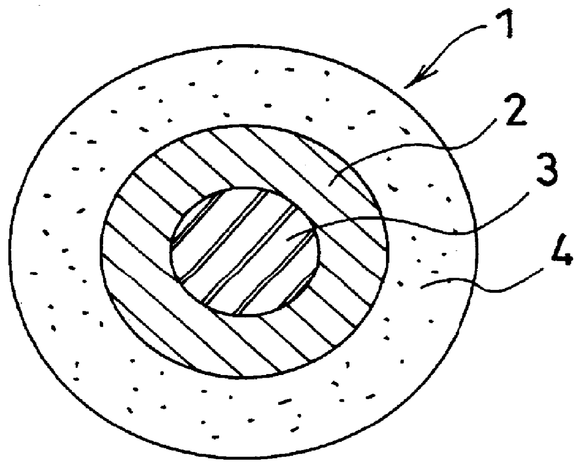
Using the manufacturing furnace of Example 1 for carrying out the Czochralski method which was capable of growing a 6" .PHI. single crystal, a single crystal was further pulled. The growth of the single crystal was made in two hot zones A, B wherein the maximum pulling rate was likewise at 1.8 mm / minute in hot zone A and at 1.4 mm / minute in hot zone B. After a single crystal was grown under the same conditions as in example 1 except the rotation rate of the crucible, the state of occurrence of defects in the crystal was checked in the same manner as in example 1.

FIGS. 6A and 6B are, respectively, views showing the distribution of defects of Example 2 in the same manner as in Example 1, in which FIG. 6A shows the defect distribution of the crystal grown in hot zone A and FIG. 6B shows the defect distribution of the crystal grown in hot zone B. The interstitial oxygen concentration in the crystals was found to be at 8.5 to 10.0.times.10.sup.17 atoms / cm.sup.3. The state of occurrence o...


PUM

PropertyMeasurementUnit
melting pointaaaaaaaaaa
temperatureaaaaaaaaaa

Abstract

A silicon single crystal wafer having good device characteristics can be manufactured according to the Czochralski method without formation of any dislocation cluster within a crystal surface. Where a silicon single crystal having an oxygen concentration of less than 8.5x10¹⁷ atoms / cm3 (ASTM F1188-88) is manufactured, a radius of a latent zone of oxidation induced stacking defects ring-likely-distributed in the crystal surface is made within a range of 70% to 0% of a crystal radius, and a value of V / G (mm2 / DEG C.xminute) is controlled at a predetermined critical value or over at radial positions except an outermost periphery of the crystal when a pulling rate is taken as V (mm / minute), and a crystalline temperature gradient along the pulling axis is taken as G ( DEG C. / mm). On the other hand, when a silicon single crystal having an oxygen concentration of not less than 8.5x10¹⁷ atoms / cm3 (ASTM F1188-88) is manufactured, a pulling rate is further set at 1.0 mm / minute or over. In the method for manufacturing the silicon single crystal wafer, it is preferred to calculate the crystalline temperature gradient G along the pulling axis through heat transfer calculation, set the critical value of V / G at 0.20 mm2 / DEG C.xminute, and control the value of V / G at a value larger than the critical value.

Description

This invention relates to a method for making a silicon single crystal suitable for use as a semiconductor device, and more particularly, to a method for making a high-quality silicon single crystal wafer which is substantially free of any harmful grown-in defects.DESCRIPTION OF THE PRIOR ARTFor the growth of a silicon single crystal used as a semiconductor material, many methods are known, among which the Czochralski method has now been in wide use. When subjected to thermal oxidation treatment (e.g. under conditions of 1000 to 1200.degree. C..times.1 to 10 hours) in an oxidative atmosphere, the silicon single crystal wafer made according to the Czochralski method may, in some cases, have ring likely distributed oxidation induced stacking faults hereinafter referred to simply as OSF ring). The zone where the OSF ring latently occurs or breaks out is influenced by the pulling rate (mm / minute) of a single crystal being grown. When the pulling rate is decreased, the zone where the OSF...

Claims


Application Information

Patent Timeline
Patent Type & Authority Patents(United States)
IPC IPC(8): C30B15/00C30B15/20C30B29/06H01L21/208
CPCC30B15/203C30B29/06
Inventor HORAI, MASATAKAEGASHIRA, KAZUYUKITANAKA, TADAMI
Owner SUMITOMO MITSUBISHI SILICON CORP
Why Eureka
Try Eureka