

Image sensor producing at least two integration times from each sensing pixel
a technology of image sensor and sensing pixel, applied in the field of semiconductor image sensor, can solve the problems of ccds being susceptible to damage from both ionizing and displacement damage, presenting engineering difficulties in manufacturing, and ccds being susceptible to displacement damage caused by high-energy particles and photons, so as to improve the flexibility and performance of the system
- Summary
- Abstract
- Description
- Claims
- Application Information
AI Technical Summary
Benefits of technology
Problems solved by technology
Method used
Image

Examples
embodiment 200
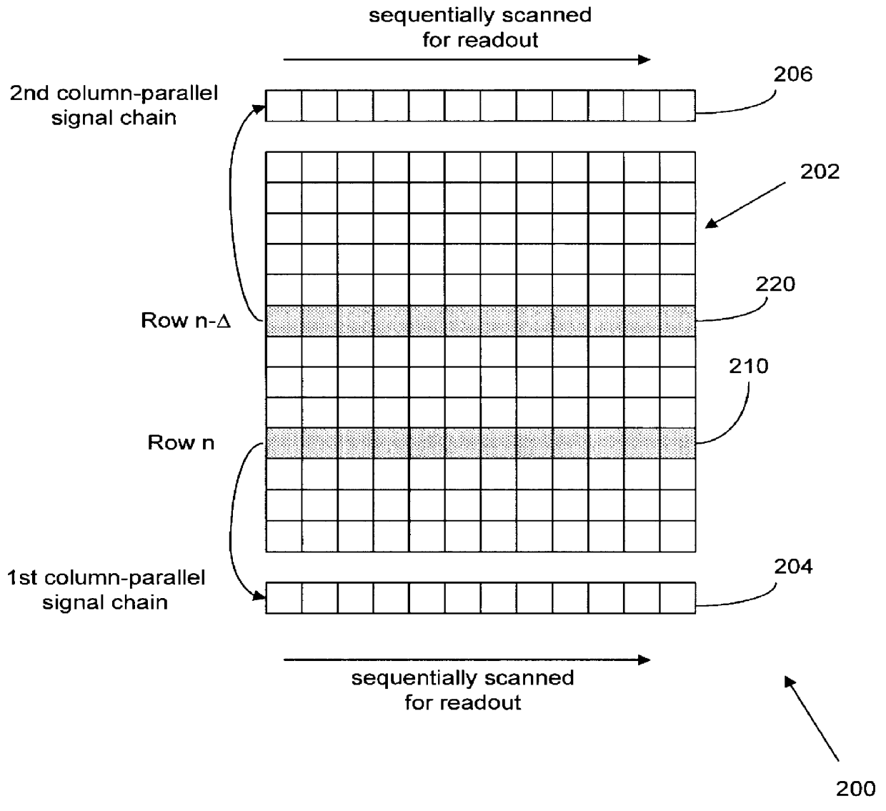
FIG. 2 illustrates the first preferred embodiment 200 of the present invention. An active pixel array 202 has N rows and M columns, hence with a total of N.times.M pixels. Each pixel comprises a light sensing element and one or more active transistors. The active transistors amplify and buffer the signals generated by the light sensing element in the pixel. Each active pixel has one output source follower that is connected to the corresponding column bus. There are two column-parallel signal chains for readout. Each of the signal chains, 204 and 206, has M storage cells for temporarily storing the electrical signals from the pixels being read. The column-parallel signal chains 204 and 206 can be implemented with capacitor banks for analog processing and analog-to-digital converters (ADCs) for digital processing or any other device that is capable of storing image information.
The device 200 also includes an control circuit (not shown) having row and column decoders for addressing the...
second embodiment
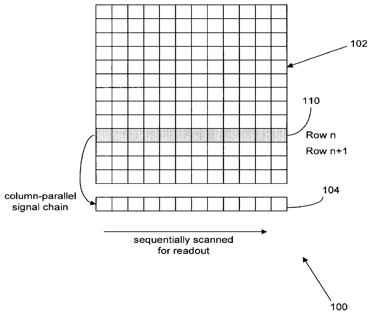
the present invention uses the readout technique for the system 200 of FIG. 2 in the system 100 of FIG. 1 to extend the dynamic range. The readout sequence is illustrated in FIG. 4. The row n of pixels 110 in the active pixel array 102 is first selected for readout. The signals in the M pixels of the row n 110 are then copied simultaneously to the corresponding M storage cells in the column-parallel signal chain 104. The copying process also resets the pixels in the row n 110 and begins a new integration in the row n 110. Subsequently, the M storage cells of the column-parallel signal chain 104 is sequentially scanned and the signals therein are read out. Next, the signals of M pixels of another row(n-.DELTA.) 402 are simultaneously copied to the corresponding M storage cells in the column-parallel signal chain 104. The row 402 is displaced from the row 110 by .DELTA. number of rows. The pixels in the row (n-.DELTA.) 402 are subsequently reset for another integration. Subsequently, ...
third embodiment
A third embodiment implements more than two integration times in an active pixel array. For a number of k integration times (k>1) for each active pixel, the respective integration times are T.sub.1int =k.DELTA..sub.1 T.sub.row, T.sub.2int =k .DELTA..sub.2 T.sub.row, . . . , and T.sub.kint =k(N-.DELTA..sub.1 -.DELTA..sub.2 . . . -.DELTA..sub.k-1)T.sub.row, if the architecture 100 of FIG. 1 is used in which there is only one column-parallel signal chain for readout. The respective readout time for a frame is T.sub.frame =NkT.sub.row. For example, N=585 and k=4, .DELTA..sub.1 may be chosen to be 1, .DELTA..sub.2 =8, .DELTA..sub.3 =64 so that T.sub.1int =1.times.4T.sub.row, T.sub.2int =8.times.4T.sub.row, T.sub.3int =64.times.4T.sub.row, and T.sub.2int =512.times.4T.sub.row.
In addition, k column-parallel signal chains can be implemented and used in a similar way as in the first embodiment 200. k rows of pixels are read out simultaneously and stored in the k column-parallel signal chains...
PUM
 Abstract
Description
Claims
Application Information