
Junction mott transition field effect transistor (JMTFET) and switch for logic and memory applications

Inactive Publication Date: 2000-09-19
IBM CORP
View PDF4 Cites 149 Cited by
  • Summary
  • Abstract
  • Description
  • Claims
  • Application Information

AI Technical Summary

Benefits of technology

Hence, the present device provides a Junction Field Effect Transistor, in which the gate insulator is a depletion layer within doped silicon. However, it is similar to the conventional MTFET and thus easy to manufacture, in that the gate insulator merely differs from STO by the presence of an ionized dopant.
The Junction-type structure is well adapted to function in an inversion mode, where the carrier polarity in the channel material, whose dopant concentration in this case would be low, is inverted by the gate potential (e.g., from p-type as normal in cuprates to n-type). Operating in the inversion mode, a good on / off ratio would be obtained without requiring extremely thin layers of channel material.

Problems solved by technology

However, practical considerations such as manufacturing reliability may impose a scaling limit before these physical limits are reached.
However, a problem encountered with the use of high dielectric constant materials as gate insulators in both capacitor applications and in MTFET devices is that, when the gate insulator becomes very thin, to achieve switching with 1-2 volt gate signals, the dielectric constant tends to rapidly decrease.
This prevents achieving desired turn-on gate voltages.
These devices are typically formed by deposition of cuprate layers on to pre-deposited STO gate oxide film, but it is recognized that this process may limit the control of quality at the cuprate-STO interface, which is the most critical part for device performance.

Method used


Image

  • Junction mott transition field effect transistor (JMTFET) and switch for logic and memory applications
  • Junction mott transition field effect transistor (JMTFET) and switch for logic and memory applications
  • Junction mott transition field effect transistor (JMTFET) and switch for logic and memory applications

Examples


Embodiment Construction

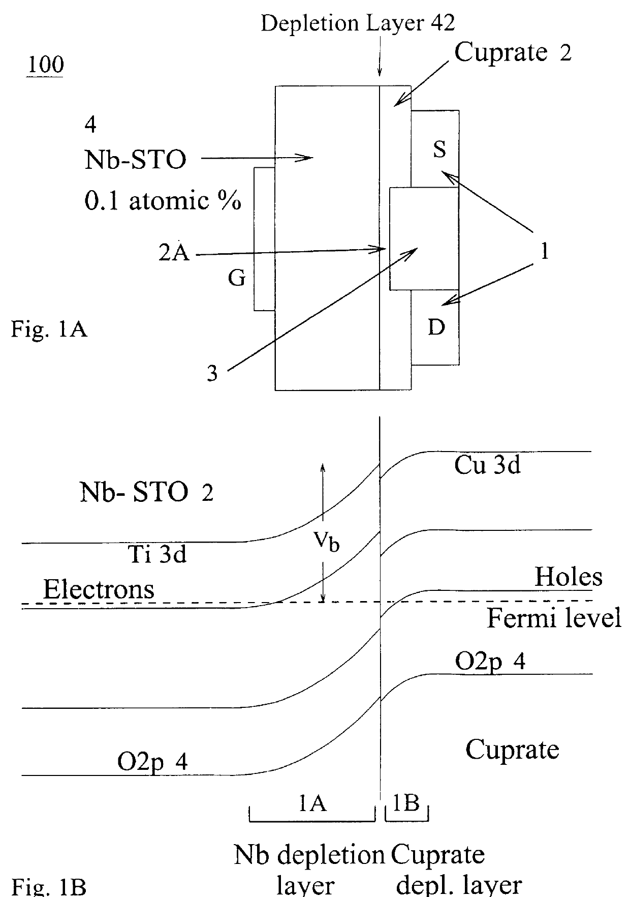
Referring now to the drawings, and more particularly to FIGS. 1A-1B, there are shown embodiments of the method and structures according to the present invention.

Generally, the present invention provides a JMTFET in which the gate insulator is essentially the same material as the gate insulator in the MTFET, with the exception that it contains a small (e.g., about 0.01 to about 10%) percentage of dopant atoms.

Referring to FIG. 1A, an embodiment of the present invention is shown and specifically one form of the JMTFET device 100 is illustrated.

First and second contacts 1 (e.g., source and drain electrodes S, D) are separated by an active channel material 2 selected for its capability to undergo the Mott metal-insulator transition. For example, the channel material 2 may be p-type channel material (e.g., Y.sub.0.5 Pr.sub.0.5 Ba.sub.2 Cu.sub.3 O.sub.7-.delta., YBa.sub.2 Cu.sub.3 O.sub.7-.delta., LaCuO.sub.4+.delta., and the like). Preferably, the contacts are formed of metal such as pla...


PUM


Abstract

A device includes first and second contacts formed on a channel material, a film of doped first insulator material interposed between the first and second contacts, and a second insulator material interfaced with the doped first insulator material with an area of said channel material therebetween. The second insulator material is doped so as to have carriers of opposite charge to those in the channel material.

Description

1. Field of the InventionThe present invention generally relates to a thin film electronic component, and more particularly to a very thin film junction Mott transition field effect transistor (JMTFET), a dynamic random access memory (DRAM) incorporating the same, and a method of forming the JMTFET.2. Description of the Related ArtDisregarding issues of lithography, the continuation of Moore's Law in scaling of digital circuits reaches a threshold when the dimensions of the MOSFET reaches the physical limits of the device.Recently, a 60 nm. channel length has been announced as constituting this limit, which may be reduced further by technical advances such as dual gate technology and the like. However, practical considerations such as manufacturing reliability may impose a scaling limit before these physical limits are reached.The function of the Si-based MOSFET is based on the presence in the channel of the device of a pair of back-to-back p-n junctions, each with an associated dep...

Claims


Application Information

Patent Timeline
IPC IPC(8): H01L49/00H01L21/70H01L21/8242H01L27/108
CPCH01L49/003H01L27/10873H10N99/03H10B12/05H10B12/00
Inventor NEWNS, DENNIS MERTON
Owner IBM CORP
Features
  • Generate Ideas
  • Intellectual Property
  • Life Sciences
  • Materials
  • Tech Scout
  • Unparalleled Data Quality
  • Higher Quality Content
  • 60% Fewer Hallucinations
Learn More