Booster circuit for semiconductor device

a semiconductor device and booster circuit technology, applied in semiconductor devices, instruments, apparatus without intermediate ac conversion, etc., can solve the problems of large influence of back-gate bias characteristics, tendency can be canceled, and long booster tim

Inactive Publication Date: 2000-09-19
RENESAS ELECTRONICS CORP
View PDF6 Cites 41 Cited by
  • Summary
  • Abstract
  • Description
  • Claims
  • Application Information

AI Technical Summary

Problems solved by technology

Thus, the boosting time becomes long.
However, when the frequencies of the drive signals #1 to #4 become high, such a tendency can be canceled.
However, in the conventional booster circuits, as the boosted voltage becomes high, the influence of back-gate bias characteristics becomes large.
Thus, the boosting efficiency deteriorates.
In addition, on the final output side, the current supplying capability and thereby the boosting efficiency deteriorate.
As is clear from FIG. 20, as the number of stages becomes large, the current supplying capability of the booster circuit deteriorates and the boosted voltage is limited
When the number of transfer transistors connected in series and the number of charge pumps connected in parallel are varied, a circuit that controls the switch becomes complicated.
In addition, the layout area becomes large.

Method used


Image

  • Booster circuit for semiconductor device
  • Booster circuit for semiconductor device
  • Booster circuit for semiconductor device

Examples


first embodiment

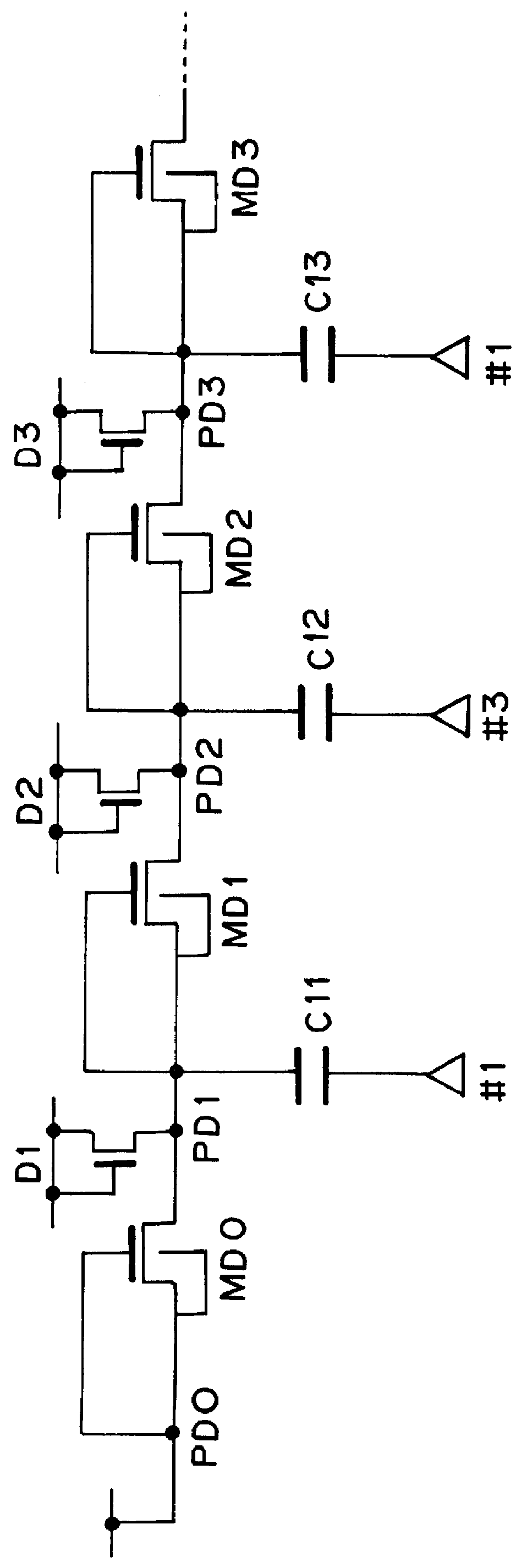
FIG. 1 shows the structure of a first embodiment of the present invention. The circuit structure of the first embodiment is the same as the circuit structure of the related art reference shown in FIG. 18.

In FIG. 1, booster cells comprise transfer transistors MD0 to MD3, capacitors C11 to C13, and MOS transistors D1 to D3. An input terminal, a drain, and a gate of each transfer transistor are connected. A source of each transfer transistor is an output terminal. A first terminal of each capacitor is connected to the source of each transfer transistor. A clock signal is supplied to a second terminal of each capacitor. A drain, a gate, and a power supply of each MOS transistor are connected. A source of each MOS transistor is connected to the source of each transfer transistor. A plurality of booster cells are tandem-connected. A power supply Vcc is supplied to the input terminal of the booster cell in the first stage.

Each of the transfer transistors MD0 to MD3 of the booster cells is ...

second embodiment

Next, a second embodiment of the present invention will be described. In a four-phase clock booster circuit as shown in FIG. 5, the current supplying capability, the boosting efficiency, and the boosting speed are superior to those in the two-phase clock type booster circuit shown in FIG. 1.

The circuit structure of the booster circuit shown in FIG. 5 is basically the same as that shown in FIG. 1. In other words, transfer transistors MJn and transfer transistors NJn are triple-well transistors. A drain of each of the transfer transistors MJn and the transfer transistors NJn is connected to a relevant sub-transfer transistor.

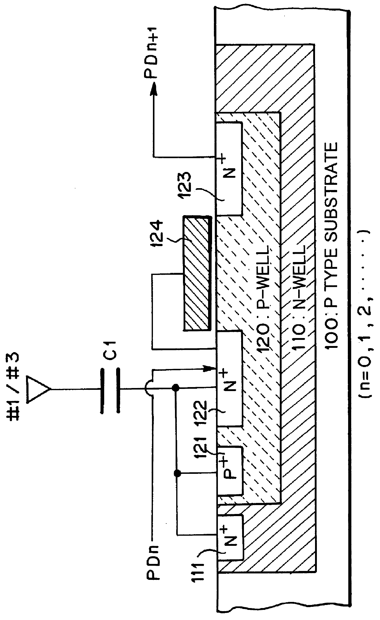
FIG. 6 is a sectional view showing a real example of the structure of each booster cell shown in FIG. 5. As shown in FIG. 6, each booster cell is composed of a triple-well semiconductor device. Each transfer transistor MJn comprises an N type first well 210 and a P type second well 220. The N type first well 210 is formed on a P type semiconductor substrate 200. T...

third embodiment

Operation of Third Embodiment

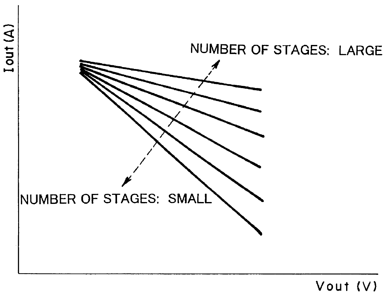
Next, the operation of the third embodiment will be described. Due to a low voltage of Vout and back-bias characteristics, at the beginning of the boosting operation, the MOS transistor MN1 is turned off. At that point, electricity for two charge pumps connected in parallel (four staged booster cells.times.2) is supplied as the final output voltage Vout.

In the middle of the boosting operation, since the voltage Vout at the output terminal P1 rises, the transistor MN1 is turned on. However, since the gate voltage is not sufficiently high, the charge transfer capability of the transistor MN1 is low. In other words, the charge pump 4 is in a transition state of which a parallel state is changed to a series state (eight staged booster cells.times.1). Thus, the current supplying capability of the booster circuit is in the middle of the current supplying capability of (four staged booster cells.times.2) and the current supplying capacity of (eight staged boost...


PUM


Abstract

A booster circuit is disclosed, the booster circuit having a plurality of booster cells tandem-connected, each of the boosters having a transfer transistor and a capacitor, an input terminal, a drain, and a gate of the transfer transistor being connected, a source of the transfer transistor being an output terminal, a first terminal of the capacitor being connected to the source of the transfer transistor, a clock signal being supplied to a second terminal of the capacitor, wherein the transfer transistor is composed of a triple-well having a first well and a second well, the first well being formed on a semiconductor substrate, the second well being formed on the first well, and wherein the semiconductor substrate is connected to a reference voltage, a diffusion layer in the first well, a first diffusion layer in the second well, a second diffusion layer in the second well, the first terminal of the capacitor, and the gate of the transfer transistor being connected, the conduction type of the first well being the same as the conduction type of the diffusion layer in the first well, the conduction type of the second well being the same as the conduction type of the first diffusion layer in the second well, the conduction type of the second well being different from the conduction type of the second diffusion layer in the second well.

Description

1. Field of the InventionThe present invention relates to a booster circuit for boosting a voltage supplied from a power supply, in particular, to a booster circuit for generating a plurality of power supply voltages, the booster circuit being disposed in for example a semiconductor non-volatile storage device.2. Description of the Related ArtConventionally, in a semiconductor non-volatile storage device, for example, an electrically erasable and programmable read only memory (EEPROM), when a signal is written thereto or erased thereto and therefrom, a booster circuit having a plurality of booster cells connected in series is used for needing the higher voltage than the power supplying voltage.Such a booster circuit is described in Japanese Patent Laid-Open Publication No. 7-111095. In the related art reference, as shown in FIG. 16, a booster circuit is composed of N type transistors formed on a P type substrate. The booster circuit shown in FIG. 1 is a two-phase clock type booster ...

Claims


Application Information

Patent Timeline
Patent Type & Authority Patents(United States)
IPC IPC(8): G11C5/14G11C16/06H02M3/07
CPCG11C5/145G11C5/14
Inventor MIKI, ATSUNORI
Owner RENESAS ELECTRONICS CORP
Why Eureka
Try Eureka