Very thin film capacitor for dynamic random access memory (DRAM)

a technology of dynamic random access memory and very thin film, applied in the direction of fixed capacitors, stacked capacitors, fixed capacitor details, etc., can solve the problem of increasing the problem of fitting the specified capacitance into the ever-decreasing specified area, the requirement of silicon technology becoming increasingly difficult to meet, and the film thickness further decreases

Inactive Publication Date: 2000-10-03
IBM CORP
View PDF7 Cites 52 Cited by
  • Summary
  • Abstract
  • Description
  • Claims
  • Application Information

AI Technical Summary

Problems solved by technology

Hence, there is an increasing problem in fitting the specified capacitance into the ever-decreasing specified area.
However, as memory densities approach 10.sup.9 bits per chip, the requirement is becoming increasingly difficult to fulfil in silicon technology, and there is a wide interest in a group of alternative materials.
This is a fundamental problem, since the reduction in dielectric constant in thin films of high dielectric constant material is widely prevalent.
Hence, as films of high dielectric constant material such as STO (strontium titanate) and BST (barium strontium titanate) are made progressively thinner with the objective of approaching realistic capacitances per unit area, a film thickness is reached where no significant further increase in capacitance results from a further decrease in film thickness, and it becomes questionable as to whether they can reach the required specification for DRAM applications.
However, at the interface between the dielectric film and one of the electrodes, dipoles do not see (e.g., are not near) any neighboring dipoles outside the interface, as there would be if the dipoles in question lay within the interior of a bulk crystal.
Another problem occurring with some perovskite dielectrics is that leakage current may be excessive, leading to an inconveniently short refresh time for the DRAM fabricated from such a material.
A further cause of the "dead layer effect" may be structural disorder at the dielectric / electrode interface.

Method used


Image

  • Very thin film capacitor for dynamic random access memory (DRAM)
  • Very thin film capacitor for dynamic random access memory (DRAM)
  • Very thin film capacitor for dynamic random access memory (DRAM)

Examples


first embodiment

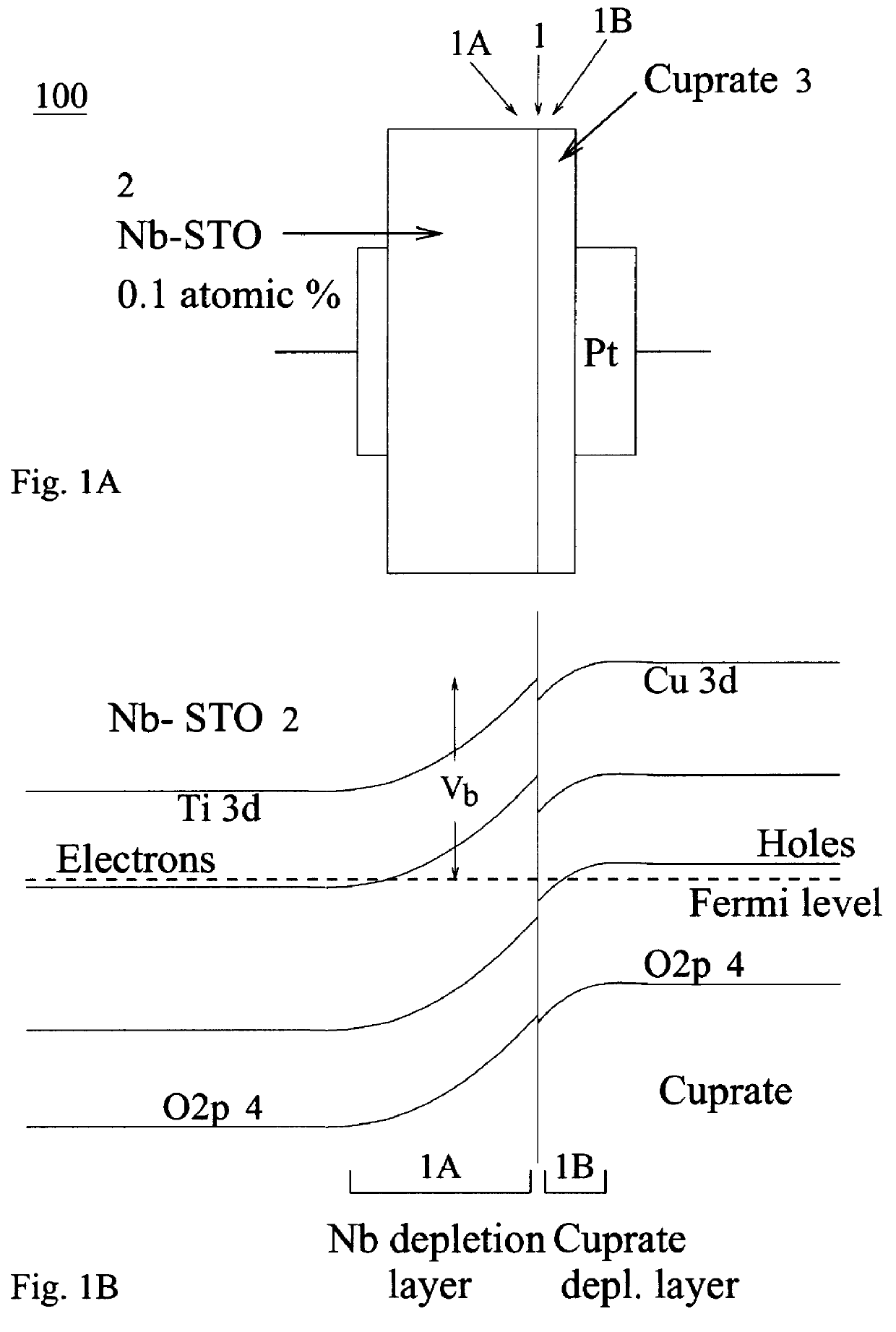
In a first embodiment of the present invention, as shown in FIGS. 1A-1B, a depletion layer structure is formed within a doped perovskite (e.g., doped Nb-STO as but one example as mentioned above).

As shown in FIG. 1A, such a structure 100 was formed using the interface 1 between a Nb-doped STO layer 2 (e.g., a 0.1% Nb-doped STO layer) and a cuprate material 3 (e.g., Y.sub.0.5 Pr.sub.0.5 Ba.sub.2 Cu.sub.3 O.sub.7), as shown in FIG. 1A.

The Nb-STO layer 2 is n-type, while the cuprate material 3 is p-type. Obviously, the conductivity of these materials could be reversed.

Assuming that at the interface 1, the oxygen bands 4 (as shown in FIG. 1B) on each side of the interface approximately line up (e.g., match), and the metal bands on each side also approximately line up (e.g., the Ti and Cu bands shown in FIG. 1B), then equalization of the Fermi levels in the two materials will cause depletion layers 1A, 1B to be formed at the interface 1. Application of the standard formula for depletion ...

second embodiment

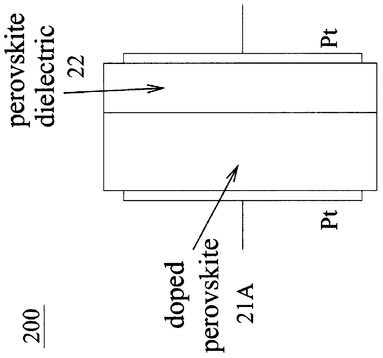
In a second embodiment of the present invention, a structure 200 as shown in FIG. 2, is provided with an electrode(Pt)-insulating perovskite 22-conducting perovskite 21A arrangement.

Structure 200 can be formed by depositing insulating perovskite 22 onto conducting perovskite 21A by laser ablation, or by ion implanting a compensating ion, such as Mg, into a conducting perovskite substrate. This embodiment shares the advantages of the first embodiment, but over a wider range of voltages for the same dielectric thicknesses.

Third Embodiment

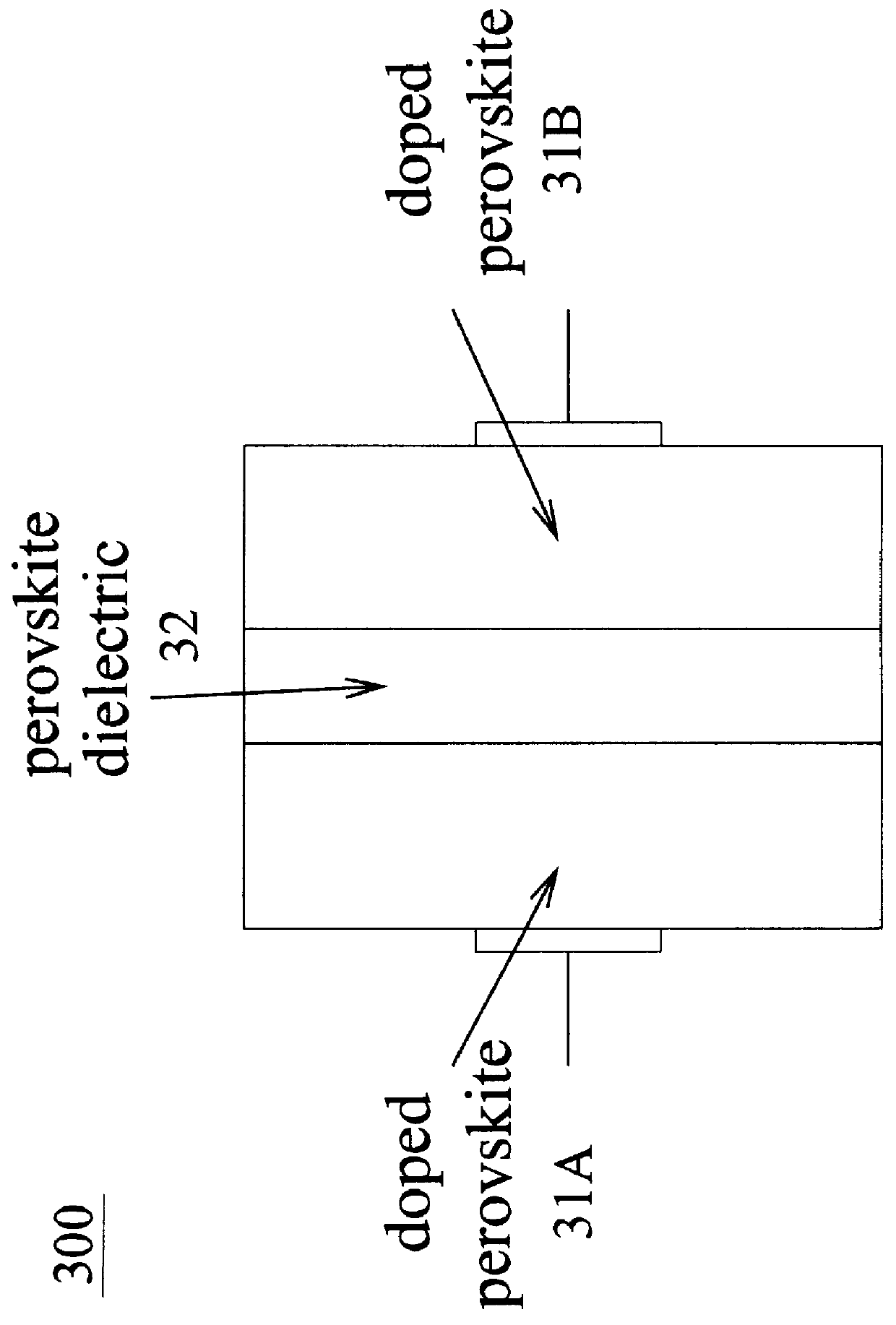
In a third embodiment of the present invention, a structure 300 as shown in FIG. 3 is formed by laser ablation, molecular beam etching (MBE) or the like (e.g., by ion implanting a compensating ion, such as Mg, into the doped material to form insulating layer 32).

Specifically, the sandwich structure 300 includes a conducting perovskite layer 31A, an insulating perovskite layer 32, and a conducting perovskite layer 31B. Such a structure may be formed, f...

third embodiment

The third embodiment includes all of the advantages of the first embodiment, but the third embodiment will be harder to fabricate but will have further advantages of having higher capacitance and being operable over a wider voltage range. Thus, the first embodiment is simpler to fabricate but the third embodiment (and the second embodiment discussed above) should work better and have higher performance.


PUM


Abstract

A capacitor and a dynamic random access memory (DRAM) incorporating such a capacitor, includes a first layer of conducting, doped perovskite material, a second layer of another conducting, doped perovskite of opposite polarity in contact with the first layer, and a depletion layer formed at an interface between the first and second layers of conducting perovskite materials, the depletion layer being an insulating layer of the capacitor. Another capacitor and DRAM incorporating such a capacitor, includes a first electrode, a second electrode opposing the first electrode, and a thin-film of high dielectric constant perovskite material sandwiched between the first and second electrodes. At least one of the first and second electrodes is formed from substantially the same perovskite material, as the thin-film, in conducting, doped form.

Description

1. Field of the InventionThe present invention generally relates to a thin film electronic component, and more particularly to a very thin film capacitor for a dynamic random access memory (DRAM) and a method of forming the same.2. Description of the Related ArtDRAM capacitors are required to store approximately 10.sup.5 electrons, but simultaneously to fit into the limited area per bit specified in the memory design. Moore's Law, whereby the density of circuits on a chip increases exponentially with time (e.g., doubling every x years) equivalently stipulates that the area per bit decreases exponentially with time (e.g., halving every x years). Hence, there is an increasing problem in fitting the specified capacitance into the ever-decreasing specified area.Current DRAM capacitors are fabricated in silicon technology, and use deep trenches or exfoliated structures to get the specified capacitance into the area per bit. However, as memory densities approach 10.sup.9 bits per chip, th...

Claims


Application Information

Patent Timeline
Patent Type & Authority Patents(United States)
IPC IPC(8): H01L21/02H01L27/04H01L21/28H01L21/822H01L21/8242H01L27/108H01L29/12H01L29/43H01L29/92
CPCH01L28/55H10B12/00
Inventor NEWNS, DENNIS MERTON
Owner IBM CORP
Why Eureka
Try Eureka