Encapsulating a solder joint with a photo cured epoxy resin or cyanate

Inactive Publication Date: 2000-10-10
ULTRATECH INT INC
View PDF24 Cites 48 Cited by
  • Summary
  • Abstract
  • Description
  • Claims
  • Application Information

AI Technical Summary

Benefits of technology

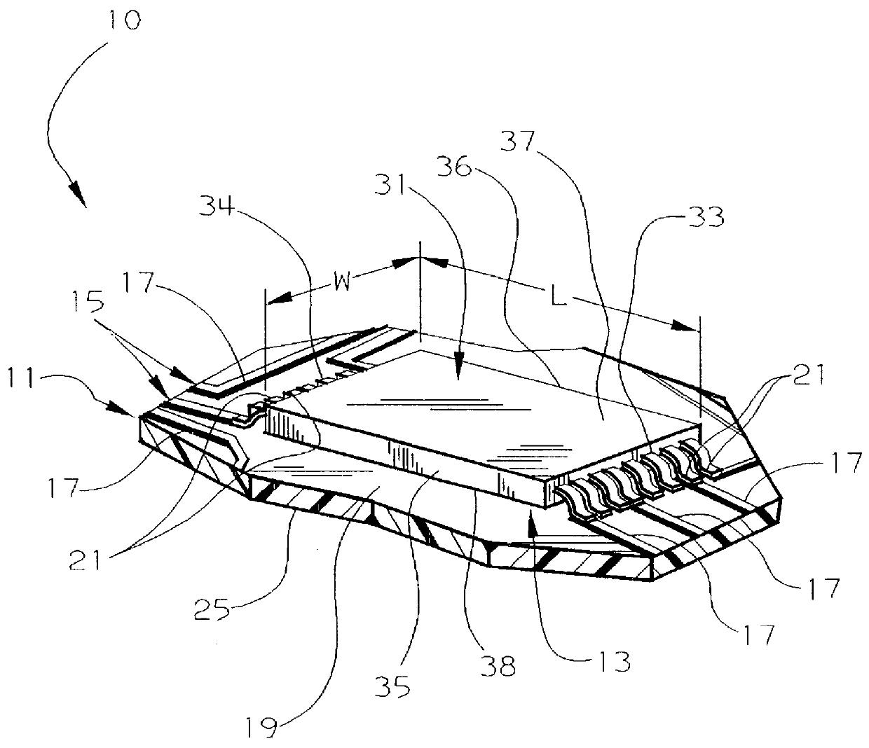
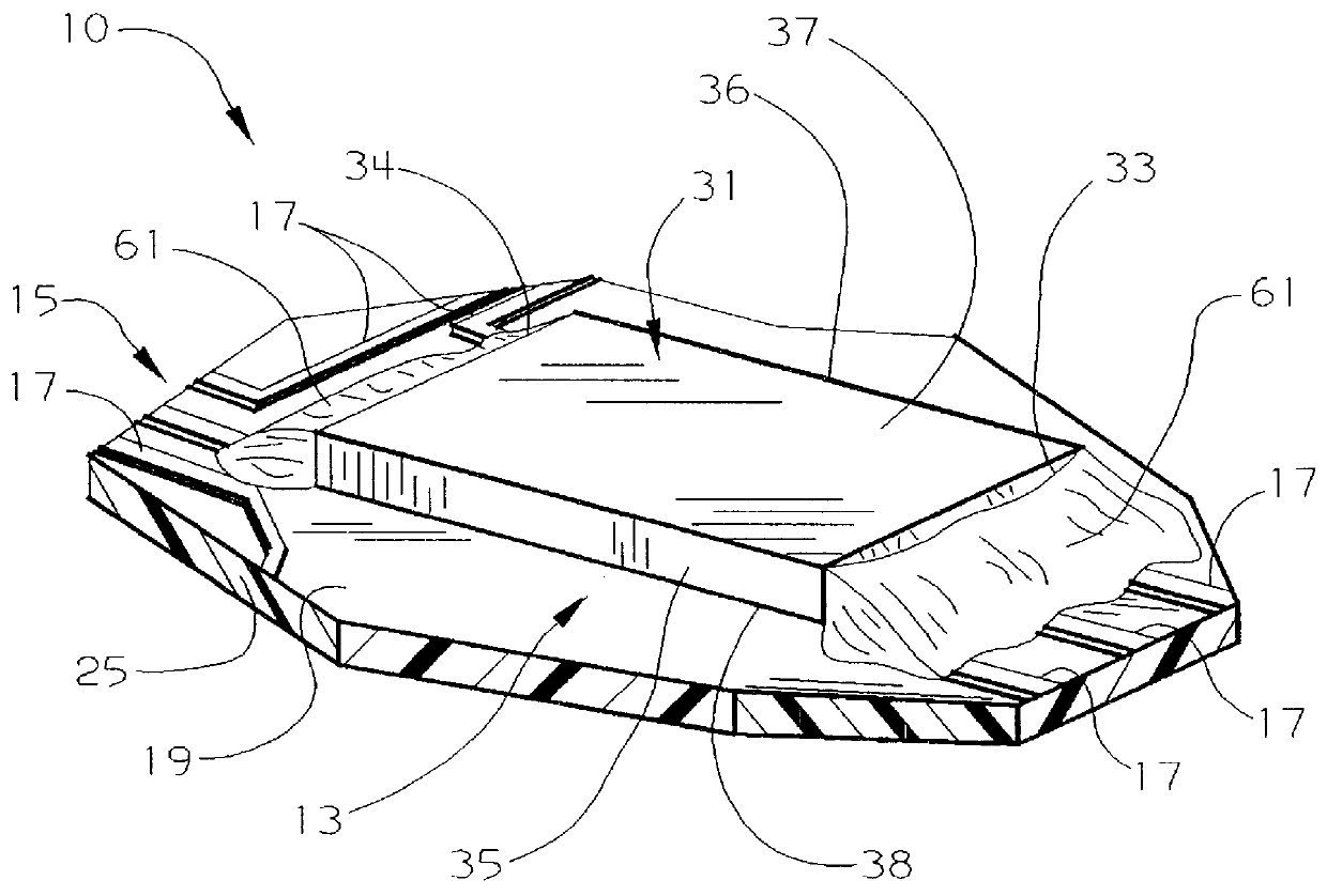
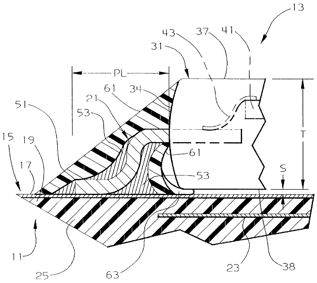
As shown in the FIGURES, a quantity of encapsulant material 61 is applied to the opposing sides 33 and 34 of integrated circuit chip housing 31 so as to abut against these sides and substantially cover the solder 53. The encapsulant material 61, as shown in FIG. 3, substantially surrounds the entire quantity of solder 53 for each of the paired lead-conductor combinations. To be noted is that the encapsulant 61 is not shown in FIG. 1. This is to enable illustration of the assembly with solder exposed. But encapsulant 61 is provided in FIG. 2. Encapsulant 61 is applied in unpolymerized form, e.g., liquid form, with a suitable photoinitiator or photocatalyst, following the solder reflow (and solder solidification) step. In a preferred embodiment, encapsulant 61 is dispensed using at least one syringe, syringe pump, or other dispenser means. This dispensing of encapsulant may occur following a pre-heating of the substrate 11 and integrated circuit chip electronic package 31 located thereon for a predetermined time period. The substrate 11 having the integrated circuit chip package 31 soldered in position thereon, is heated to drive off the moisture therein, e.g., to within a range of from about 65 degrees C to about 85 degrees C for about one to two hours. The purpose of the heating is to drive off any undesirable moisture which may collect within the dielectric material which forms part of substrate 11. A hot air oven is preferably used to accomplish this heating. Subsequently, encapsulant 61 may be dispensed while the substrate 11 retains much of the heat from this preheating step. Following encapsulant dispense, the board with mounted package and encapsulant is positioned under a source of ultra-violet (UV) radiation and subjected to UV radiation to effect polymerization, i.e., photopolymerization, of the encapsulant 61.
A pre

Problems solved by technology

It has been found that when TSOP packages, as well as similar thin packages, are surface mounted on organic substrates (and particularly those of epoxy resin or perfluorocarbon dielectric material) of relatively thick configuration (e.g., greater than about 0.050 inches thick), relatively

Method used


Image

  • Encapsulating a solder joint with a photo cured epoxy resin or cyanate
  • Encapsulating a solder joint with a photo cured epoxy resin or cyanate
  • Encapsulating a solder joint with a photo cured epoxy resin or cyanate

Examples


example 2

The following statistically designed experiment was performed to optimize depth of cure and determine the effect of various parameters. A "master" mixture was prepared by weighing 25 g of Novacup L337 silica filler into a 100 ml plastic beaker. To this was added 25 g of Union Carbide ERL-4221 cycloaliphatic resin. This was mixed by hand with a glass stirring rod to a smooth consistency. This mixture was divided into two 20 g portions. To one beaker was added 0.24 g of Union Carbide Cyracure UVI-6974 (50% mixture of photoinitiator in propylene carbonate). To the other beaker was added 2.0 g of Cyracure UVI-6974. Portions of each mixture were added to eight 30.times.30.times.4 mm aluminum caps. Each cap was exposed to a 5 mW / sq. cm. mercury lamp for the times indicated below. The caps were processed as indicated in the table. Baking was done in either a Fisher Isotemp or a Blue M oven by first bringing oven to temperature then inserting parts for time indicated. After processing the c...

example 3

A mixture of resins were prepared in a glass beaker by heating on a hot plate 1 g of Epon 1007 and 9 g of ERL-4221. The hot plate was maintained at 140-150.degree. C. for 3 hours until the Epon 1007 dissolved. While warm, 0.01 g of ethyl violet dye and then 15 g of Novacup L337 silica was added and mixed with a stir rod. The dark blue mixture was viscous when cool. The mixture was applied with a stir rod to the leads on a circuitized ceramic test substrate. The substrate was exposed for 2 minutes under the 5 mW / sq. cm. mercury lamp, then baked at 120.degree. C. for 5 minutes. The surface had hardened. The ceramic was cooled to -70.degree. C. several times in a freezer and warmed to room temperature. A crack was observed at a bubbled area in the applied material, otherwise the integrity and adhesion were good.

The set of sixteen runs carried out, with 0.5 weight percent to 5 weight percent initiator, a UV exposure dose of 30 to 180 seconds, a hold time of 0 to 2 hours, a bake temperat...

example 4

A homogeneous liquid mixture was prepared by mixing 10 g of Arocy L10 from Ciba, 0.1 g of 10% solution of 8% Zn octanoate in mineral spirits from Mooney Chemicals and 0.15 gr of Irgacure 261 from Ciba. To this solution 15 g of Novacup L337 silica was added and mixed with a stir rod.

Alternatively another mixture was prepared by adding 5 gr of Arocy L10, 5 gr of MR283-250, 0.1 gr of Zn Octanoate and 0.15 gr of Irgacure 261 were added. To this solution 17 g of Novacup L337 silica was added and mixed with a stir rod.

Each sample was roll milled for 1 hr after addition and vacuum degassed to remove the entrapped air. Coatings (2 mils) of these mixtures were first baked for 15 min at 130.degree. C., exposed for 300 sec (350 W Oriel Lamp) and baked at 150.degree. C. for 15 minutes. The resulting cured films appeared to be of good quality and do not appear to crack upon a 90 degree bend test.

The composition protects the soldered joints from the effects of thermal cycling.

Thus there has been ...


PUM

PropertyMeasurementUnit
Lengthaaaaaaaaaa
Thicknessaaaaaaaaaa
Angleaaaaaaaaaa

Abstract

An electronic package assembly where a low profile integrated circuit chip package is soldered to an organic (e.g., epoxy resin) substrate, e.g., a printed circuit board or card, the projecting conductive leads of the integrated circuit chip package and the solder which substantially covers these leads (and respective conductors on the substrate) having been substantially covered with ultraviolet photocured encapsulant material (e.g., an epoxy resin or a cyanate with a photoinitiator and silica) to provide reinforcement for the solder-lead connections. The encapsulant material is dispensed about the solder and lead joints following solder reflow and solidification so as to substantially surround the solder and any portions of the leads not covered with solder.

Description

The present invention relates to low profile electronic circuit package structures and particularly to such packages for use within light weight, portable devices.Electronic package assemblies which utilize various organic substrates (e.g., printed circuit boards comprised of epoxy resin or the like material) having one or more electronic packages surface mounted thereon are known. These electronic packages include a relatively flat housing component having therein at least one semiconductor device (integrated circuit chip). This semiconductor device is, in turn, electrically connected to various conductive leads (e.g., copper) which project therefrom. One first level package known in the art is a dual in-line package (DIP). The integrated circuit chips embedded within such integrated circuit chip packages provide various functions (e.g., memory, logic, connectivity) for the overall system. The conductive leads which project from these packages are electrically coupled to respective...

Claims


Application Information

Patent Timeline
IPC IPC(8): H05K3/28H05K3/34C08G59/18C08F2/48C08G59/00C08G59/68C08G73/02H01L23/29H01L23/31
CPCH05K3/284H05K3/3421H01L2224/48091H01L2224/48472H01L2924/00H01L2924/00014
Inventor PAPATHOMAS, KONSTANTINOS I.FUERNISS, STEPHEN JOSEPHDITTRICH, DEBORAH LYNNWANG, DAVID WEI
Owner ULTRATECH INT INC
Why Eureka
Try Eureka