Impedance control using fuses

a technology of impedance control and fuse, which is applied in the direction of digital storage, semiconductor/solid-state device details, instruments, etc., can solve the problems of inability to correct circuit problems introduced during final module build, insufficient cache memory provision, etc., to achieve lower latency, eliminate excessive capacitive and inductive loading, and improve the effect of signal quality

Inactive Publication Date: 2000-10-31
MARVELL ASIA PTE LTD
View PDF6 Cites 150 Cited by
  • Summary
  • Abstract
  • Description
  • Claims
  • Application Information

AI Technical Summary

Benefits of technology

to more tightly / closely couple memory and processor chips, by providing a novel stacked memory chip / device structure that eliminates excessive capacitive and inductive loading in single and multi-processor systems in order to achieve lower latency and higher-bandwidth operation.

Problems solved by technology

However, as processor speeds dramatically increase, provision of cache memories becomes increasingly insufficient, primarily due to input capacitance loading which is a major limiting factor.
Finally, as prior art laser fuse devices must be blown at the wafer level prior to packaging and module burn-in, stresses may be introduced onto the chip that can promote circuit fails and performance anomalies.
Laser fuses cannot be blown after circuit encapsulation and, therefore, cannot be used to correct circuit problems introduced during final module build.

Method used


Image

  • Impedance control using fuses
  • Impedance control using fuses
  • Impedance control using fuses

Examples


Embodiment Construction

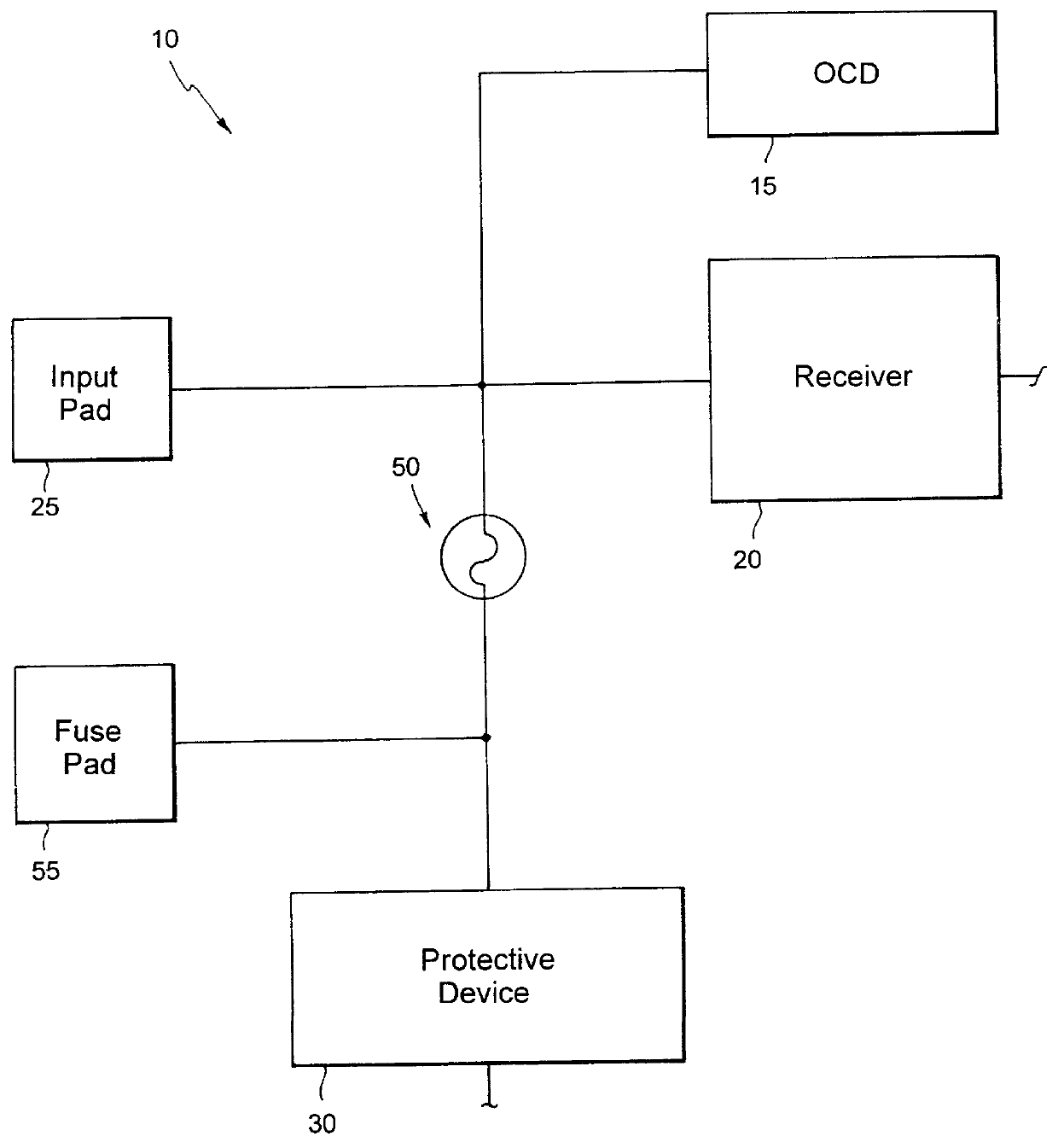
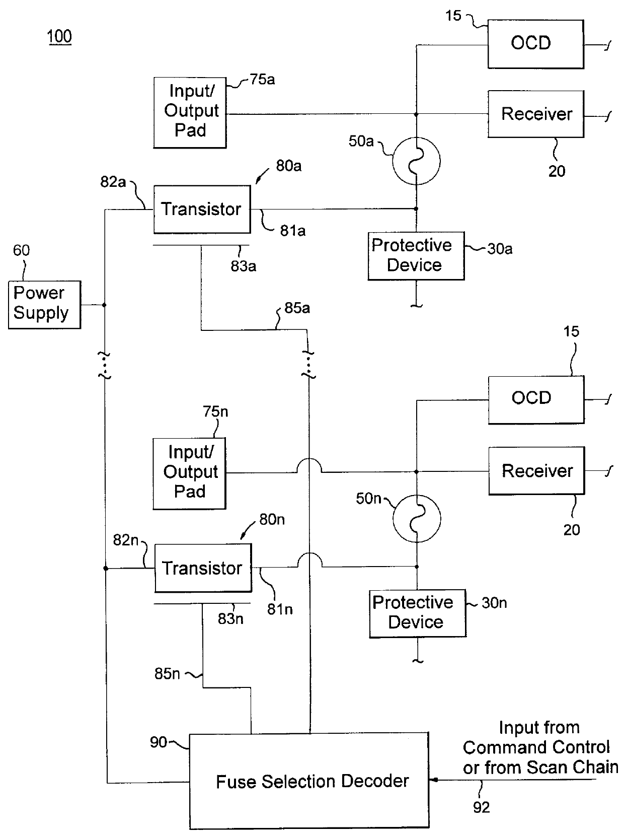
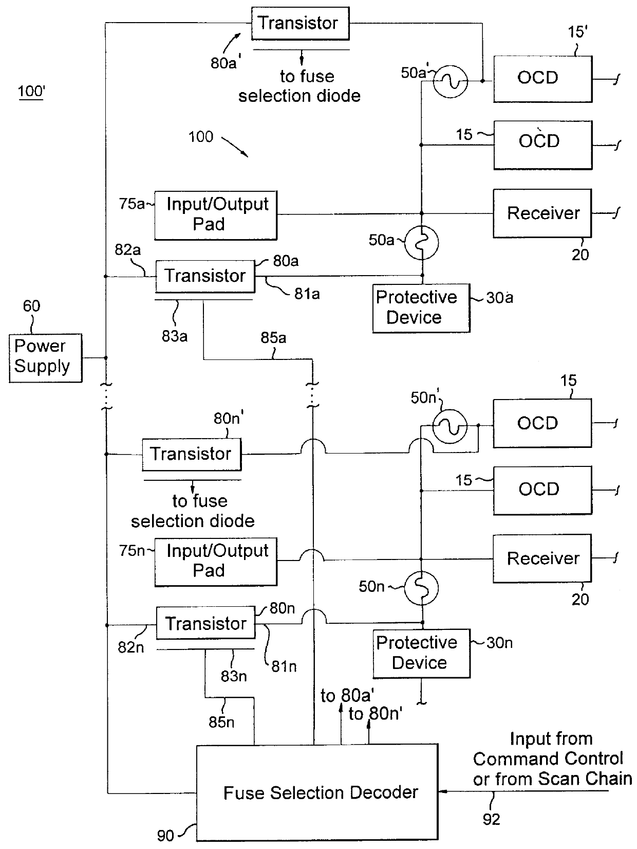
FIG. 1 illustrates a circuit structure 10 for reducing capacitive loading of a memory chip / device, e.g., a DRAM chip, having a common input / output terminal according to a first embodiment of the invention. As shown in FIG. 1, an off-chip device (OCD) 15, for example, a device for communicating to a next chip, and a receiver device 20 for receiving address / data signals from a previous chip, for example, are both connected to an input pad 25 which is the physical input for the chip. A commonly known protective device or circuit 30 is built into the structure in order to protect the receiver and OCD devices from destructive electrostatic discharge (ESD) during manufacture and handling. According to the invention, the protective device 30 is removed from the structure 10 after the chip has been placed in the final assembly, e.g., in a module or directly mounted on a substrate or printed circuit board with other chips, by positioning and subsequently opening a fuse device 50 in the struc...


PUM


Abstract

A system and method for reducing impedance loading of semiconductor integrated circuit devices implementing protective device structures that contributes to impedance loading at an I/O pad connection. The method comprises providing a fuse device between the I/O pad connection and the protective device; connecting a current source device associated with each fuse device in the integrated circuit, the current source device connected to one end of the fuse device; providing fuse selection circuit for activating current flow through a selected fuse device between the current source and the I/O connection, the current flow being of an amount sufficient for blowing the fuse and disconnecting the protective device from the circuit structure, thereby reducing impedance loading at the I/O connection. Such a system and method is employed in a memory system comprising integrated circuit chips disposed in a stacked relation, with each chip including: a layer of active circuitry formed at a first layer of each chip; a plurality of through conducting structures disposed substantially vertically through each chip for enabling electronic connection with active circuitry at the first layer; second conducting device disposed at an end of the through conducting structure at an opposite side of a chip for connection with a corresponding through conductive structure of an adjacent stacked chip, the stacked chip structure formed by aligning one or more through conducting structures and second conducting devices of adjacent chips, whereby a chip of the stack is electronically connected to active circuitry formed on other chips of the stack. The stacked chip structure is ideal for reducing data access latency in memory systems employing memory chips such as DRAM.

Description

1. Field of the InventionThe present invention relates to computer systems and memory system architectures, and specifically, to a method and apparatus for controlling device impedance loading in semiconductor circuits and device structures by implementing and selectively destructing novel fuse devices in the semiconductor chips.2. Discussion of the Prior ArtProcessor performance is increasingly gated by memory performance. Cache hierarchies are used to accommodate fast processors and fast memories. However, as processor speeds dramatically increase, provision of cache memories becomes increasingly insufficient, primarily due to input capacitance loading which is a major limiting factor. For example, memory chip devices are provisioned with protective devices which are used to protect the device from electrostatic discharge, for example, during device manufacture and handling. These protective devices can increase input capacitance by as much as 25%. For example, in a memory device ...

Claims


Application Information

Patent Timeline
Patent Type & Authority Patents(United States)
IPC IPC(8): G11C17/14G11C17/16H01L25/065H01L27/02
CPCG11C17/16H01L23/481H01L25/0657H01L2924/13091H01L2924/10253H01L2924/01019H01L2224/16H01L2225/06517H01L2225/06541H01L2225/06555H01L2225/06562H01L2225/06589H01L2225/06596H01L2924/01012H01L2924/01046H01L2924/15192H01L2924/3011H01L2924/00H01L2224/06181H01L2224/13025H01L2224/16145H01L2224/16225H01L2224/17181H01L2224/48227H01L2224/4826H01L2924/181H01L2924/00012H01L27/02
Inventor BERTIN, CLAUDE LOUISFIFIELD, JOHN A.HEDBERG, ERIK LEIGHHOUGHTON, RUSSELL J.SULLIVAN, TIMOTHY DOOLINGTOMASHOT, STEVEN WILLIAMTONTI, WILLIAM ROBERT
Owner MARVELL ASIA PTE LTD
Why Eureka
Try Eureka