Programmable impedance output buffer drivers, semiconductor devices and static random access memories provided with a progammable impedance output port

a technology of progammable impedance and output port, which is applied in the direction of logic circuit coupling/interface arrangement, digital storage, instruments, etc., can solve the problems of difficult to enable a stable operation of transistors, adversely affecting the high speed operation of semiconductor integrated circuits, and inability to realize high-speed data transmission and high-speed operation of system buses

Inactive Publication Date: 2000-10-31
KK TOSHIBA
View PDF4 Cites 24 Cited by
  • Summary
  • Abstract
  • Description
  • Claims
  • Application Information

AI Technical Summary

Problems solved by technology

In the prior art semiconductor devices, however, if there exists a mismatch between the impedance of the bus lines of the system and the impedance of the output buffer circuit of the device which is connected to the bus lines, undesirable reflection waves take place at the interface so that it is impossible to realize high speed data transmission and high speed operation of the system bus due to the reflection waves.
However, along with the decrease in the output voltage from the output pad 9 as recently required, since there results a substantial decrease in the differential voltage between the source and the drain, it is difficult to enable a stable operation of the transistors of the current mirror circuit 2 in the pentode region during an impedance matching operation conducted by controlling the on / off operation of the MOS transistors Tr constituting the pull-up dummy buffer circuit 3 or the pull-down dummy buffer circuit 5.
By this configuration, reflection waves occurs between the output pad 9 and the propagation line not shown in the figure and therefore adversely affect the high speed operation of the semiconductor integrated circuit even implemented with the programmable impedance output buffer driver.

Method used


Image

  • Programmable impedance output buffer drivers, semiconductor devices and static random access memories provided with a progammable impedance output port
  • Programmable impedance output buffer drivers, semiconductor devices and static random access memories provided with a progammable impedance output port
  • Programmable impedance output buffer drivers, semiconductor devices and static random access memories provided with a progammable impedance output port

Examples


first embodiment

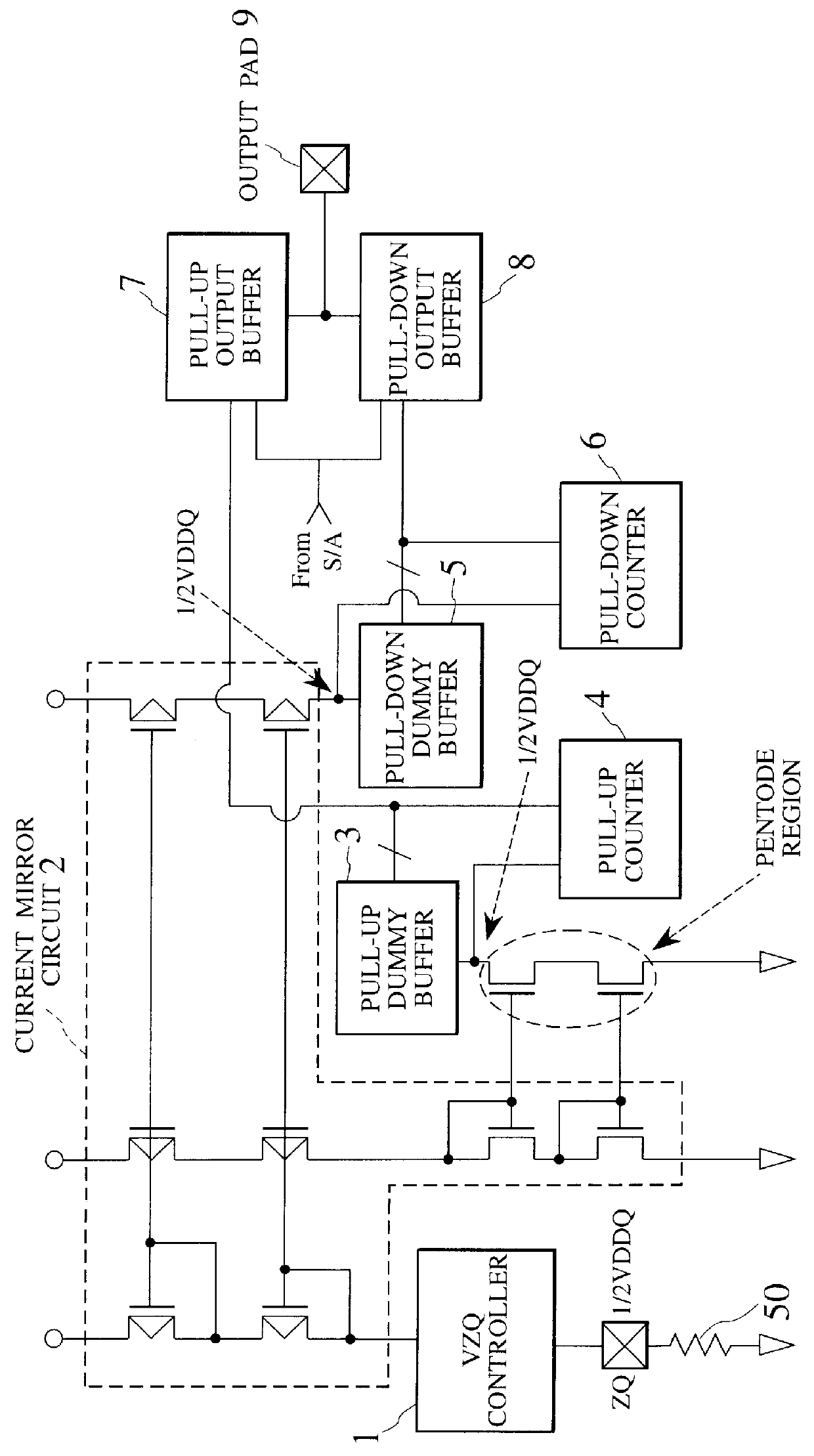
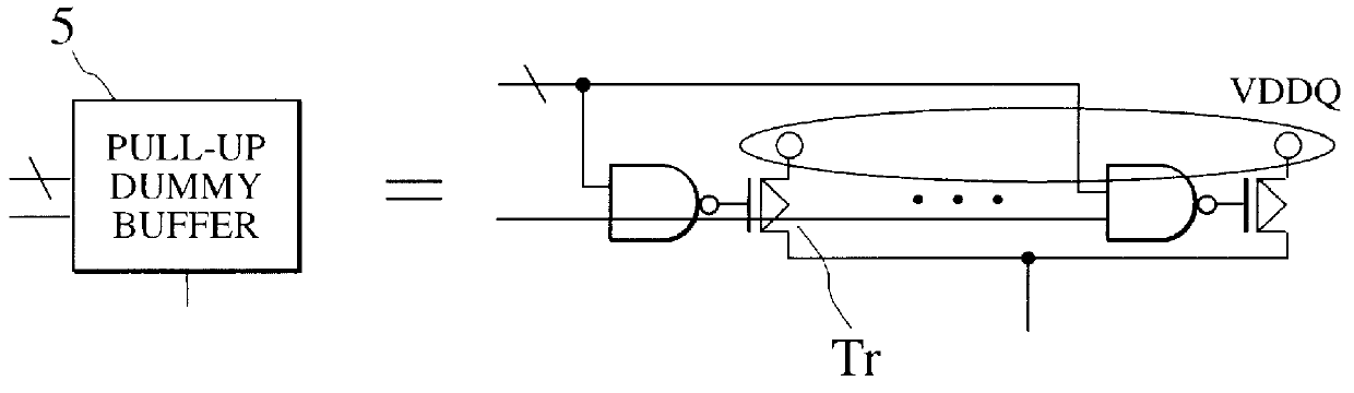
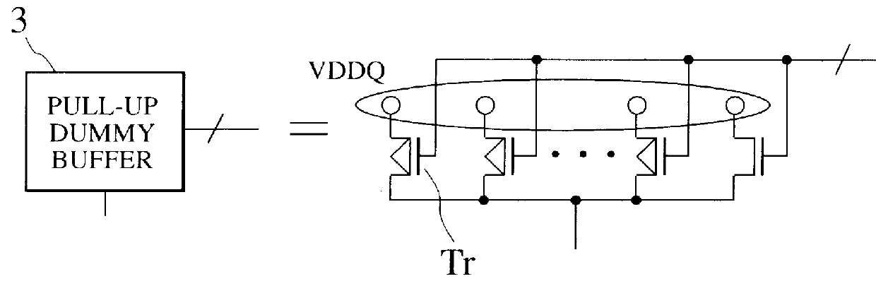
Hereinbelow, several preferred embodiments in accordance with the present invention will be explained in conjunction with the accompanied drawings. FIG. 4 is a block diagram showing a programmable impedance output buffer driver in accordance with the present invention. The programmable impedance output buffer driver includes a VZQ controller 11, a current mirror circuit 12, a first pull-down dummy buffer circuit 13, a second pull-down dummy buffer circuit 14, a pull-up dummy buffer circuit 15, a pull-down counter 16, a pull-up counter 17, a pull-up output buffer circuit 18, a pull-down output buffer circuit 19, a pad 20 and the pad ZQ. An off-chip resistor 50 selected by a user is connected between the pad ZQ and the ground. The VZQ controller 11 serves to control the potential level of the pad ZQ to be VDDQ / 2, which is a half of the output voltage VDDQ. The current mirror circuit 12 is connected to the VZQ controller 11 and the off-chip resistor 50 in series between the power volta...

third embodiment

FIG. 7 is a block diagram showing a programmable impedance output buffer driver in accordance with the present invention. Also in the drawing, like reference numbers indicate identical or functionally similar elements as the programmable impedance output buffer driver as illustrated in FIG. 6 and therefore redundant explanation is not repeated. In this embodiment of the present invention, while the impedance of the pull-up dummy buffer circuit 23 is fixed, the pull-up counter 17 is used to adjust the impedance of the pull-down dummy buffer circuit 22 to the fixed impedance of the pull-up dummy buffer circuit 23.

For example, it is assumed that, when the impedance of the pull-down dummy buffer circuit 22 is adjusted to the fixed impedance W of the pull-up dummy buffer circuit 23, the channel width of the pull-down dummy buffer circuit 22 is adjusted to .beta.W by means of the adjustment operation of the pull-up counter 17. In this case, the ratio 1 / .beta. is transferred to the multipl...

second embodiment

The impedance of the pull-up output buffer circuit 18 is then controlled to be equal to the resistance value of the off-chip resistor 50 in the same manner as the present invention as illustrated in FIG. 6.

The programmable impedance output buffer driver in accordance with the present invention is possibly effective, when used in point-to-point connection, in order to further increase the operation speed.

FIG. 8 is a circuit diagram showing a static random access memory in the form of a semiconductor large-scale integrated circuit chip as connected to one of two data ports of a processor as an example of a point-to-point connection. In this case, the programmable impedance output buffer driver in accordance with the present invention is formed also in said one of two data ports of the processor as well as in the output signal of the static random access memory. The other of the two data ports of the processor is connected to a common bus on which a plurality of DRAMs are connected In ...


PUM


Abstract

The impedance of a pull-down output buffer circuit is adjusted to an integer multiple of the resistance value of an off-chip resistor with reference to the adjustment information obtained by adjusting the impedance of the pull-down dummy buffer circuits 13 and 14 to the resistance value of the off-chip resistor by means of a pull-down counter. The impedance of the pull-up output buffer circuit is adjusted to the pull-down dummy buffer circuit 14, i.e., an integer multiple of the resistance value of an off-chip resistor with reference to the adjustment information obtained by adjusting the impedance of the pull-up dummy buffer circuit to the impedance of the pull-down dummy buffer circuit 14 by means of a pull-up counter.

Description

The subject application is related to subject matter disclosed in the Japanese Patent Application No.Hei10-353444 filed in Dec. 11, 1998 in Japan, to which the subject application claims priority under the Paris Convention and which is incorporated by reference herein.1. Field of the InventionThe present Invention is related to an improvement of The programmable impedance output buffer driver and the semiconductor device such as a static random access memory provided with a programmable impedance output buffer driver for adjusting the impedance of the output buffer circuit of the semiconductor device.2. Description of the Related ArtIn the recent years, along with increasing frequencies of input / output operations in the field of the semiconductor integrated circuits, it becomes increasingly important to avoid matching problems caused between the impedance of an output buffer circuit and the impedance of a transmission line formed on a printed circuit board (PCB).In the prior art sem...

Claims


Application Information

Patent Timeline
Patent Type & Authority Patents(United States)
IPC IPC(8): G11C7/10G11C11/417G11C11/401G11C11/409H03K19/0175
CPCG11C7/1051
Inventor KAWASUMI, ATSUSHI
Owner KK TOSHIBA
Why Eureka
Try Eureka