Method of fabricating semiconductor read-only memory device with reduced parastic capacitance between bit line and word line
- Summary
- Abstract
- Description
- Claims
- Application Information
AI Technical Summary
Problems solved by technology
Method used
Image

Examples
Embodiment Construction
FIGS. 4A through 4D are schematic sectional diagrams depicting the steps involved in the method according to the present invention for fabricating a ROM device.
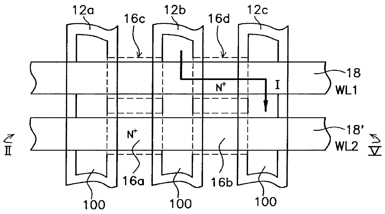
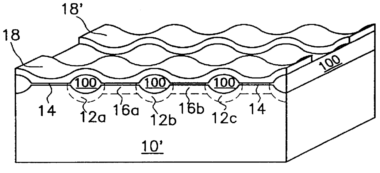
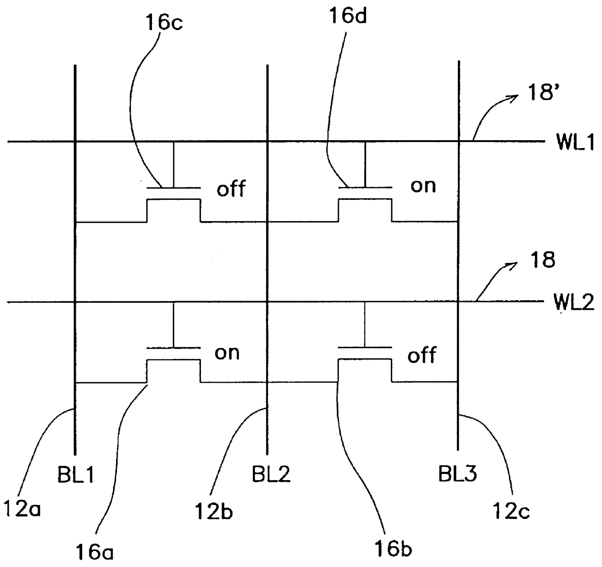
Referring first to FIG. 4A, in the first step, a semiconductor substrate, such as a P-type silicon substrate 20, is prepared. Subsequently, a conventional photolithographic and etching process is performed to form a photoresist layer 21 having a plurality of predefined openings 23 located at those positions where the bit lines of the ROM device are to be formed. By using the photoresist layer 21 as a mask, an ion implantation process is then performed on the wafer so as to diffuse an N-type impurity material, such as arsenic or phosphorus ions, through the openings 23 in the photoresist layer 21 into the exposed regions of the P-type silicon substrate 20. As a result of this, a plurality of substantially parallel-spaced N.sup.+ diffusion regions 26a, 26b, and 26c are formed, which serve as a plurality of bit lines BL1, BL2, B...
PUM
 Abstract
Description
Claims
Application Information
 - R&D
- Intellectual Property
- Life Sciences
- Materials
- Tech Scout
- Unparalleled Data Quality
- Higher Quality Content
- 60% Fewer Hallucinations
Browse by: Latest US Patents, China's latest patents, Technical Efficacy Thesaurus, Application Domain, Technology Topic, Popular Technical Reports.
© 2025 PatSnap. All rights reserved.Legal|Privacy policy|Modern Slavery Act Transparency Statement|Sitemap|About US| Contact US: help@patsnap.com