
Depth profile metrology using grazing incidence X-ray fluorescence

a grazing incidence and depth profile technology, applied in the field of measurement techniques, can solve the problems of affecting the accuracy of the reflected probe beam, the inability to meet the requirements of being an inexpensive, non-destructive technique requiring little maintenance, and the destructive nature of the sims

Inactive Publication Date: 2001-01-09
ADVANCED MICRO DEVICES INC
View PDF4 Cites 52 Cited by
  • Summary
  • Abstract
  • Description
  • Claims
  • Application Information

AI Technical Summary

Problems solved by technology

For example, as the thickness of a film varies, the intensity of the reflected probe beam also varies due to the variation in interference effects created at the interface between the thin film and the substrate.
However, SIMS does not meet the requirements of being an inexpensive, non-destructive technique requiring little maintenance, having the ability to serve as a portable monitoring station.
Although SIMS depth resolution, lateral resolution, and sensitivity continue to improve as technology advances, several drawbacks are inherent with SIMS measurements.
The biggest drawback is SIMS character as a destructive technique.
Thus SIMS is not feasible for usage as a bench-top process control station for monitoring the amount of material embedded within a substrate.
Furthermore, SIMS is a very bulky, complex, expensive method that employs complicated, maintenance-intensive machinery.

Method used


Image

  • Depth profile metrology using grazing incidence X-ray fluorescence
  • Depth profile metrology using grazing incidence X-ray fluorescence
  • Depth profile metrology using grazing incidence X-ray fluorescence

Examples


Embodiment Construction

)

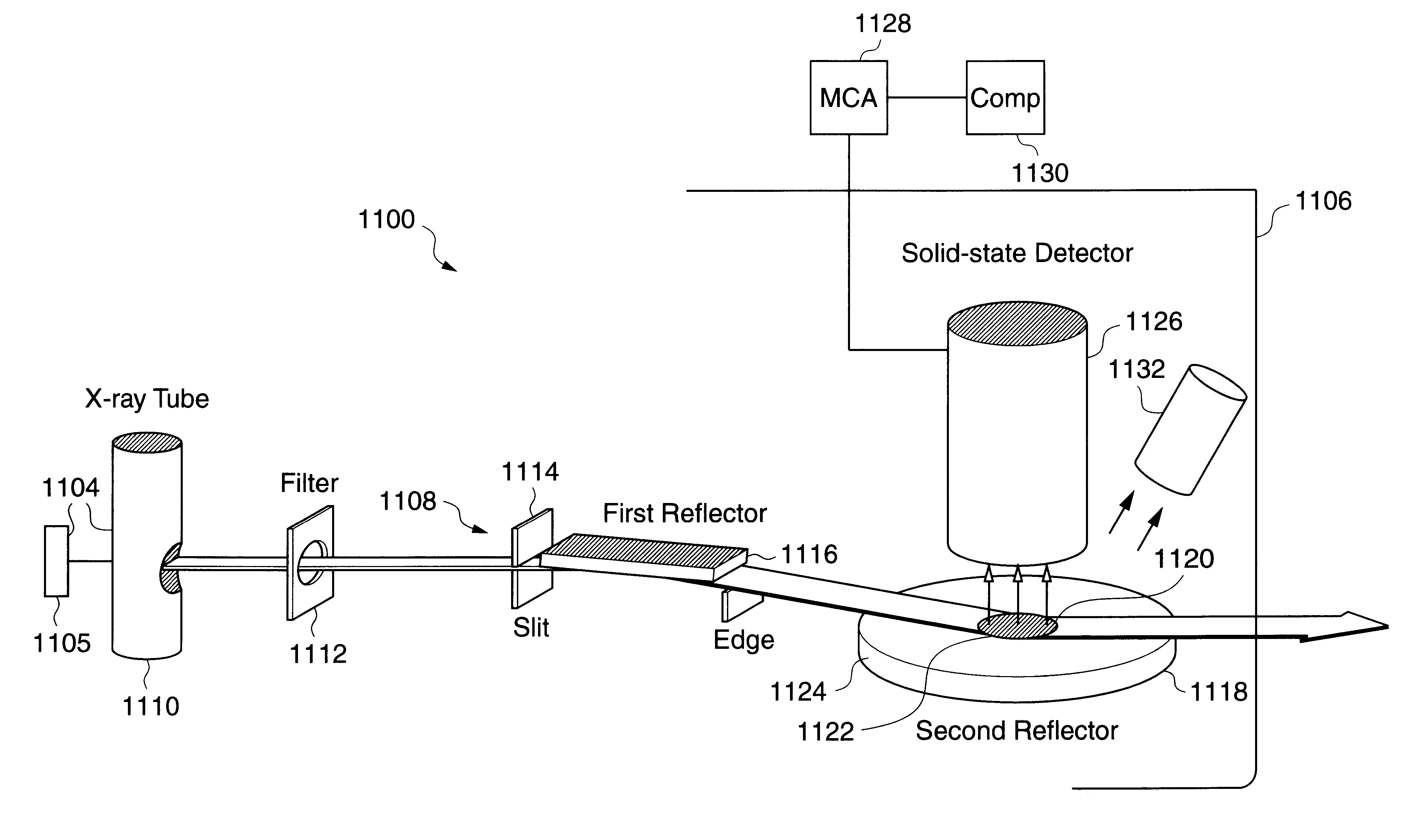
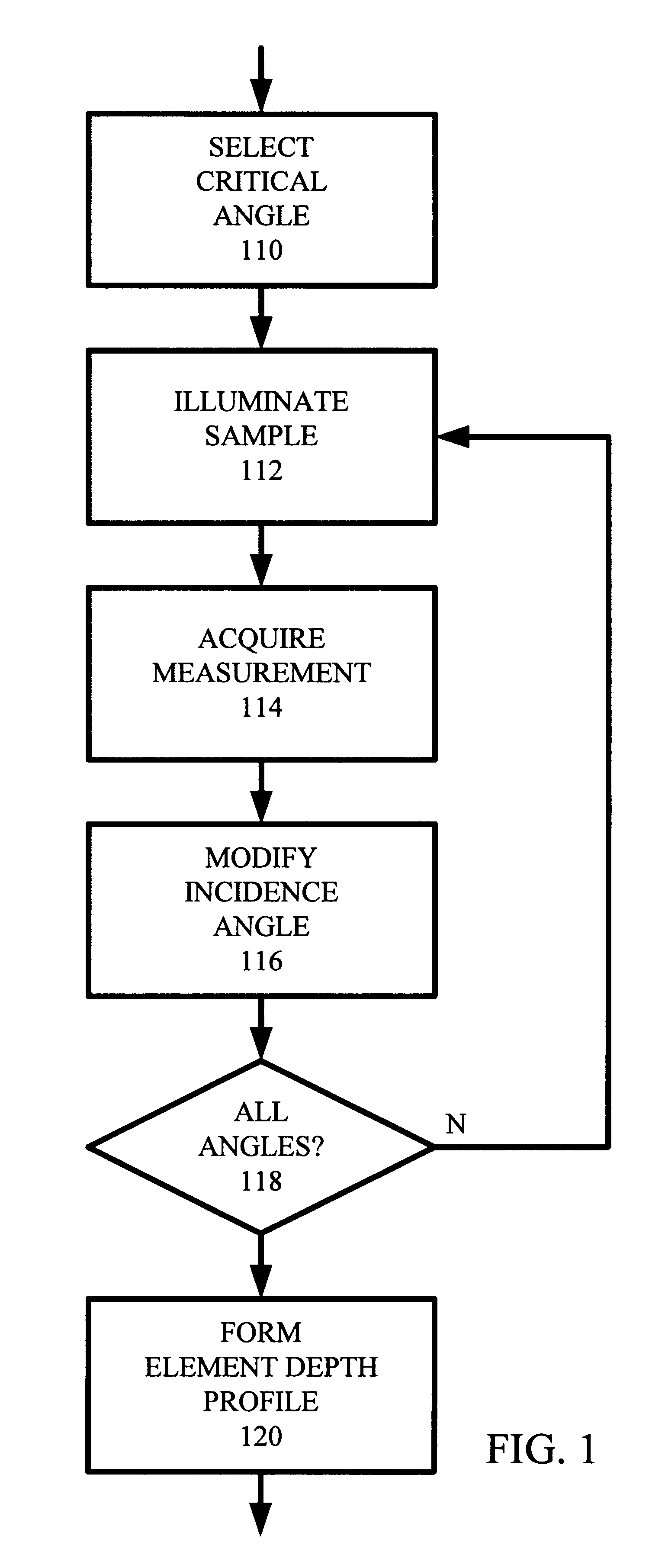
Referring to FIG. 1 a schematic flow chart that illustrate a method for determining depth profiles and implant dose for a selected element. A primary incident X-ray beam has excellent depth resolution at small angles near a critical angle of total reflection .phi..sub.crit that is selected according to the material to be analyzed in a select critical angle operation 110. In one application, X-ray fluorescence measurements are performed to profile the depth of a dopant used in semiconductor manufacturing such as arsenic, phosphorus, and boron. An X-ray beam is employed to illuminate a substrate sample at a selected incident angle that is a small angle near the critical angle .phi..sub.crit in an illuminate sample operation 112. An X-ray fluorescence measurement is acquired at the selected incident angle and stored in an acquire measurement operation 114. Following acquisition of a sample, the angle of incidence is modified in preparation for a subsequent sample in a modify incidence...


PUM


Abstract

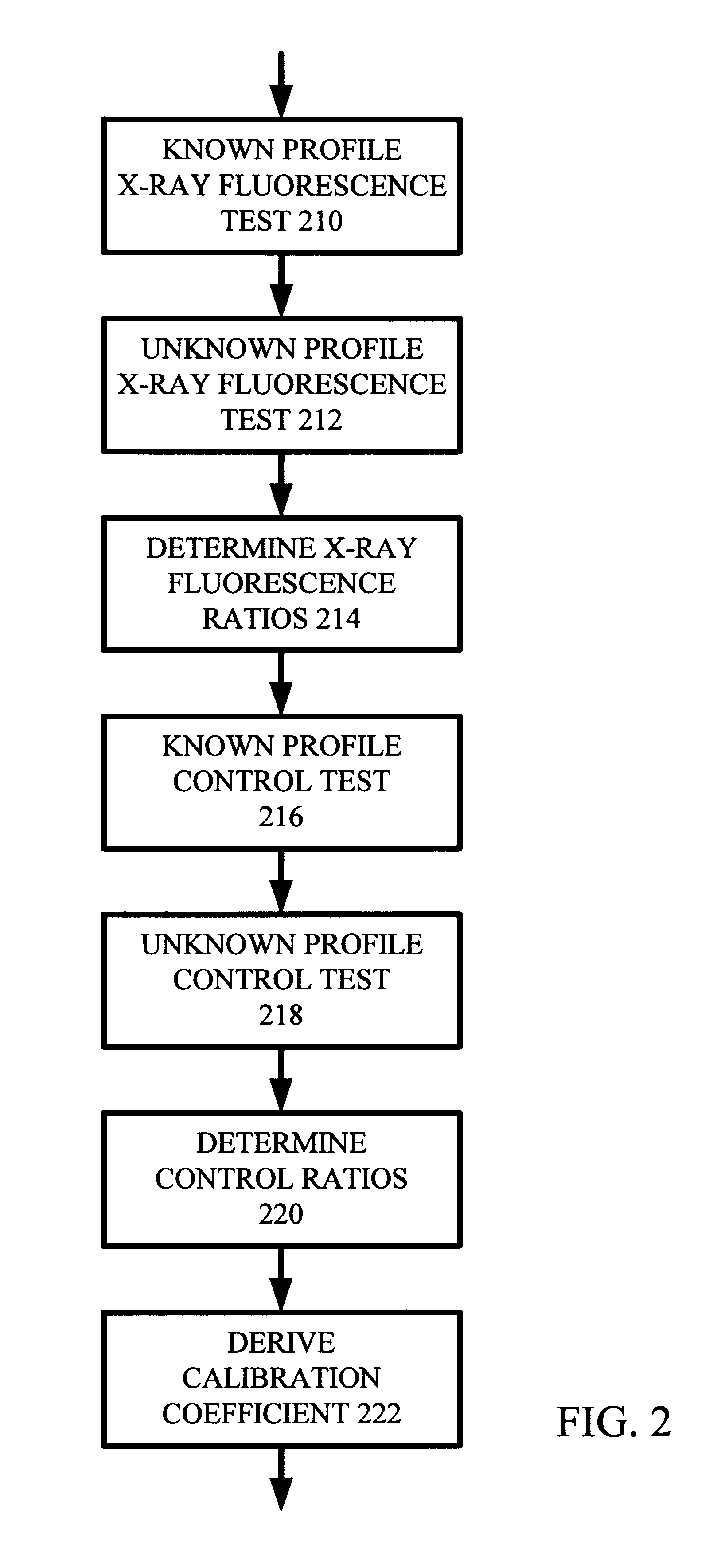
For small angles that are near critical angle, a primary incident X-ray beam has excellent depth resolution. A series of X-ray fluorescence measurements are performed at varying small angles and analyzed for depth profiling of elements within a substrate. One highly useful application of the X-ray fluorescence measurements is depth profiling of a dopant used in semiconductor manufacturing such as arsenic, phosphorus, and boron. In one example, angles are be varied from 0.01° to 0.20° and measurements made to profile arsenic distribution within a semiconductor wafer. In one embodiment, measurements are acquired using a total reflection X-ray fluorescence (TXRF) type system for both known and unknown profile distribution samples. The fluorescence measurements are denominated in counts / second terms and formed as ratios comparing the known and unknown sample results. The count ratios are compared to ratios of known to unknown samples that are acquired using a control analytical measurement technique. In one example the control technique is secondary ion mass spectroscopy (SIMS) so that the count ratios from the TXRF-type measurements are compared to ratios of integrals of SIMS profiles. In another example, the TXRF-type measurement ratios are compared to simulation profiles of known samples. Integrals of the SIMS profile that vary as a function of depth into the substrate correspond to the grazing incidence angles of the TXRF-like measurement and respective count rates.

Description

1. Field of the InventionThe present invention relates to measurement techniques used in semiconductor processing and fabrication. More precisely, the present invention relates to nondestructive measurement techniques for determining implant dose in semiconductor devices.2. Description of the Related ArtIn semiconductor processing and fabrication arts, considerable investment has been made in developing high resolution measurement devices and techniques for evaluating sample parameters. Many various types of measurements are performed in the semiconductor industry where very thin films, such as oxides, metals or dielectrics, are deposited on semiconductor substrates such as silicon. Non-destructive techniques are particularly useful for evaluating thickness, impurities and index of refraction characteristics of the films to insure high yields during fabrication.One type of information that is particularly useful in semiconductor fabrication is information relating to the dose and pr...

Claims


Application Information

Patent Timeline
IPC IPC(8): G01N23/22G01N23/223
CPCG01N23/223G01N2223/076
Inventor HOSSAIN, TIM Z.TIFFIN, DON A.WEISS, CORNELIA A.
Owner ADVANCED MICRO DEVICES INC
Learn More