Wavelength dividing circuit

a technology of dividing circuit and waveguide path, applied in the direction of optical waveguide light guide, nanotechnology, instruments, etc., can solve the problems of increasing device size, reducing crosstalk, and placing limitations on the bending radius of each waveguide path, so as to improve device characteristics or performance, the effect of high integration

Inactive Publication Date: 2001-02-13
NEC CORP
View PDF2 Cites 50 Cited by
  • Summary
  • Abstract
  • Description
  • Claims
  • Application Information

AI Technical Summary

Benefits of technology

However, in the course of the investigations toward the present invention the following problems have been encountered. Namely, the above-described conventional AWG device has the following disadvantages.
It is therefore an object of the present invention to provide a wavelength dividing circuit suitable for high integration through reduction in the device size and improved device characteristics or performance, such as high speed or high transmission efficiency.

Problems solved by technology

The first problem is the increased device size.
The reason is that a waveguide path needs to be provided separately in each path of light, with there being placed limitations on the bending radius of each waveguide path.
The second problem resides in difficulties met in reducing the crosstalk.
The reason is that leakage of optical signals occurs to a certain extent unavoidably even if the differential refractive index between a core and a clad constituting a waveguide channel is increased, while the waveguide pitch cannot be set to a sufficiently large magnitude because of the above-mentioned device size limitations.

Method used


Image

  • Wavelength dividing circuit
  • Wavelength dividing circuit
  • Wavelength dividing circuit

Examples


examples

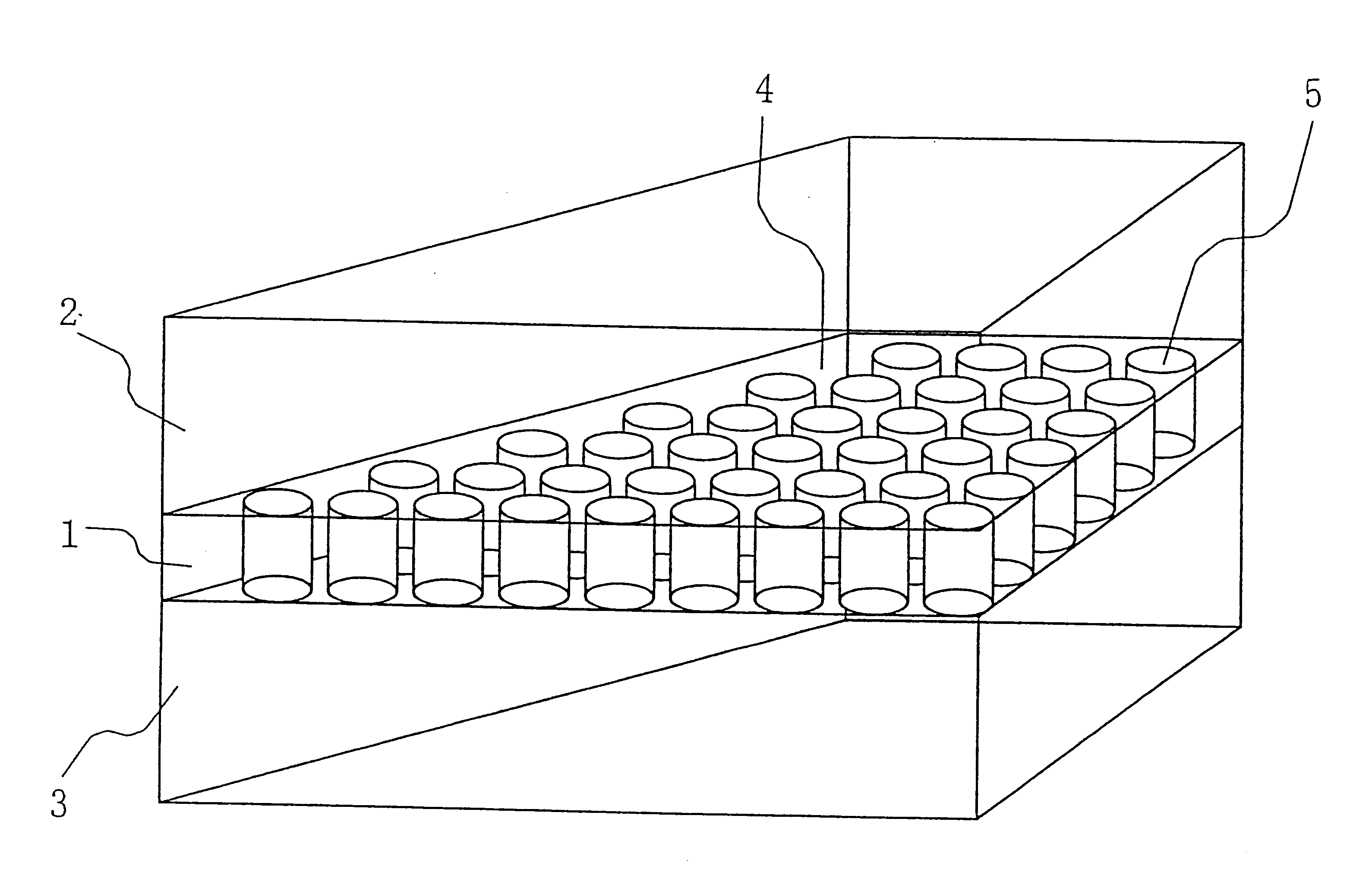
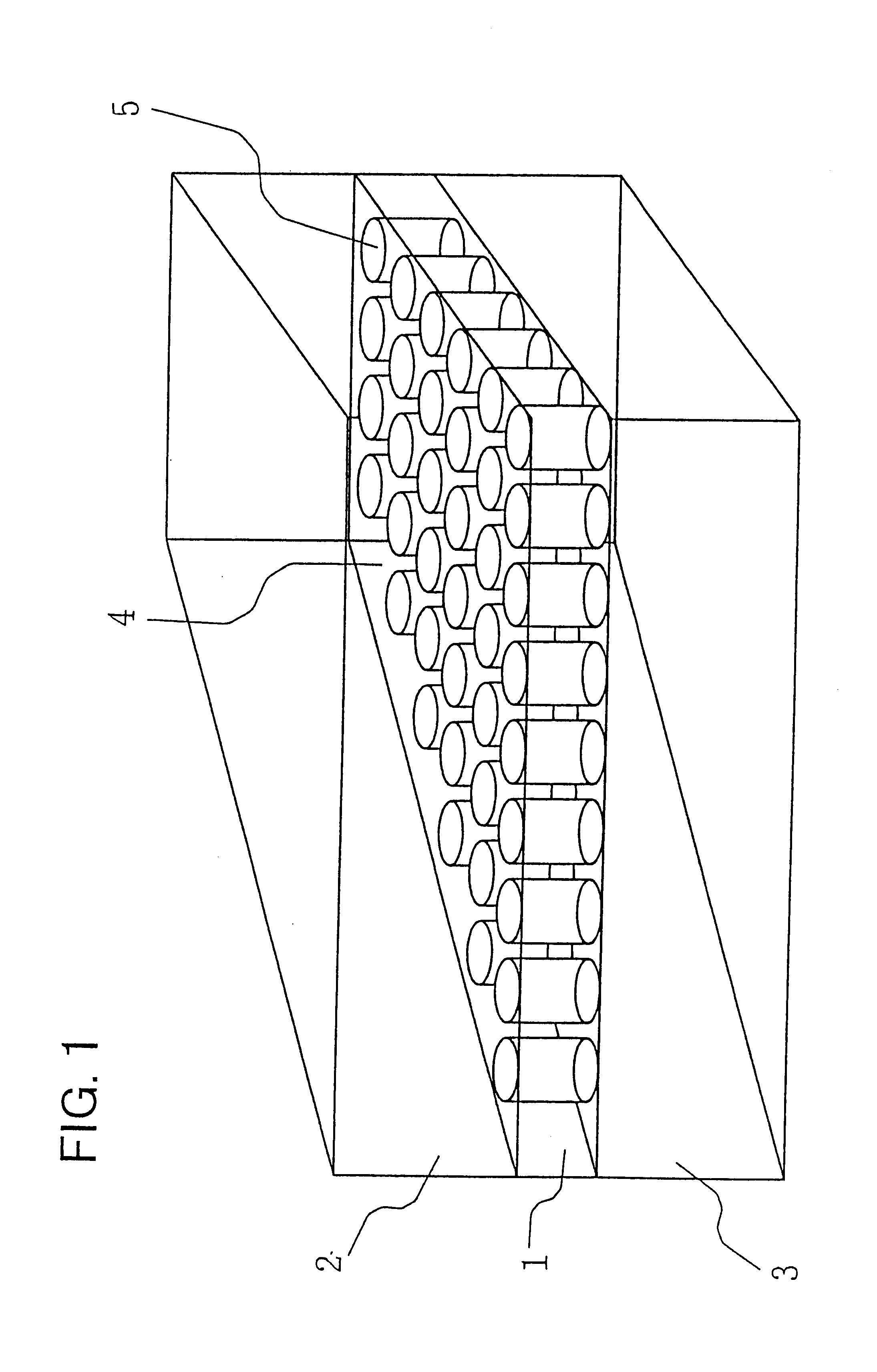
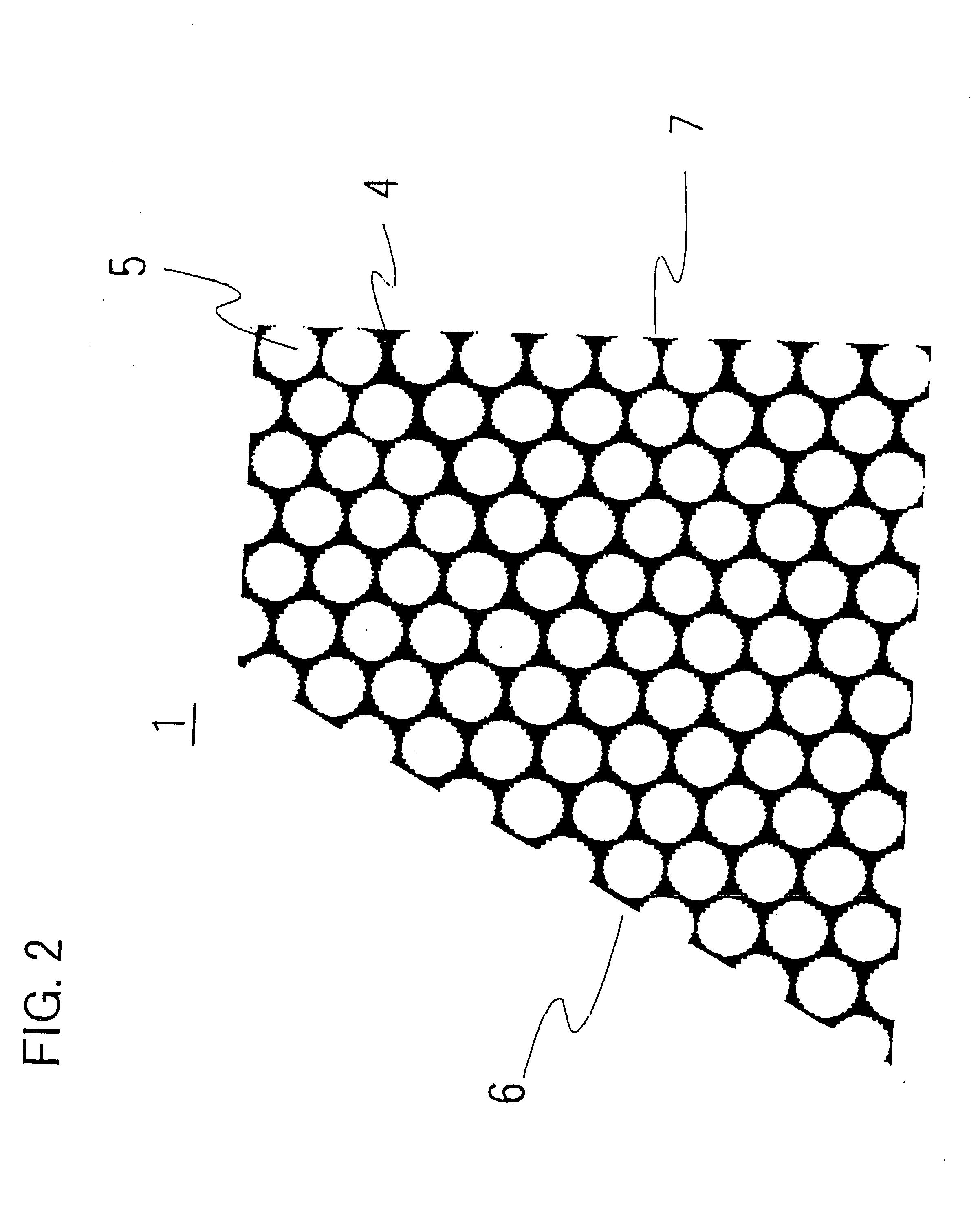
Referring to the drawings, preferred examples for carrying out the present invention are explained. FIG. 3, showing an example of the present invention, shows a substrate as a sectional view taken in a plane parallel to the substrate surface facing the clad. Meanwhile, the overall structure of the wavelength dividing circuit embodying the present invention is the same as that shown in FIG. 1.

Referring to FIG. 3, a background medium 4 and atomic is mediums 5 in the substrate 1 are silicon (Si) and air, respectively. That is, the substrate 1 is a Si substrate having through-holes.

The substrate 1 has a thickness of 1.9 .mu.m, with the atomic mediums 5 each being round columnar in shape. The openings are each 0.77 .mu.m in diameter, with an aspect ratio being 2.6. With this aspect ratio, the through-holes representing the atomic mediums 5 can be produced also by an etching process. The arraying pitch of the atomic mediums 5 is 0.83 .mu.m.

On both sides of the substrate 1, SiO.sub.2 plate...


PUM


Abstract

A wavelength dividing circuit which realizes improved device characteristics and performance, such as a small size, high speed and high transmission efficiency and which lends itself to improved integration degree. A wavelength dividing circuit in which materials of different refractive indices are arrayed periodically, without forming individual waveguides as in conventional AWG, in order to create strong wavelength dispersion characteristics not possible with an ordinary optical crystal to control wavelength deviation. A substrate 1 having atomic mediums 5 buried in a background medium 4 in a two-dimensional triangular array has its both sides sandwiched by a first clad 2 and a second clad 3. Optical signals fall on an incident surface inclined at a certain angle relative to the light incident direction and is radiated from a light outgoing surface 7. The interval between neighboring atomic mediums 5 is designed in meeting with the wavelength of the optical signals, while the thickness of the substrate 1 is designed so that the optical signals are sufficiently confined in the substrate 1 and so that the light proceeding direction is not significantly deviated from the substrate surface.

Description

This invention relates to an optical integrated circuit and, more particularly, to a planar type optical integrated circuit used in optical communication or optical control and which may be used with advantage for wavelength multiplexing optical transmission system.In the waveform multiplexing optical transmission system, a device is indispensable which splits plural wavelength multiplexed signal light beams into separate wavelength light beams, or which combines plural signal light beams into a sole wave guide path. As a device having such functions, a device employing an array waveguide lattice, referred to hereinafter as array wave guide (AWG), is felt to be promising. As an example of the AWG, a planar structure of an AWG disclosed in Takahashi et al, Meeting Abstracts to Autummn Meeting of the Society of Electronic Information Communication, Vol.4, page 272, is shown in FIG. 13.In this AWG element, shown in FIG. 13, a quartz based light guide path is formed on a waveguide subst...

Claims


Application Information

Patent Timeline
Patent Type & Authority Patents(United States)
IPC IPC(8): G02B6/122G02B6/12
CPCB82Y20/00G02B6/1225
Inventor KOSAKA, HIDEOKAWAKAMI, SHOJIRO
Owner NEC CORP
Why Eureka
Try Eureka