Optical waveguide isolator

a technology of optical waveguide and isolator, which is applied in the direction of optical elements, instruments, semiconductor lasers, etc., can solve the problems of complex manufacturing steps, high manufacturing cost, and inability to manufacture known optical waveguide isolators with semiconductor optical elements

Inactive Publication Date: 2001-03-27
THE UNIV OF TOKYO
View PDF5 Cites 57 Cited by
  • Summary
  • Abstract
  • Description
  • Claims
  • Application Information

AI Technical Summary

Problems solved by technology

The above well known optical waveguide isolator was not able to be manufactured with a semiconductor optical element such as semiconductor lasers and optical modulators as one body, since the well known optical waveguide isolator does not have the semiconductor device structure.
Therefore, the well known optical waveguide isolator must be made as another discrete structure with the substrate of the optical circuit to which the semiconductor device such as semiconductor lasers is integrated, so that the manufacturing step becomes complicated and the manufacturing cost becomes expensive, too.
Particularly, since the phase matching is necessary, and a precise processing is necessary, so that the manufacturing process becomes complex.
As a result, a complicated structure for the phase matching and precise processing step become unnecessary.

Method used


Image

  • Optical waveguide isolator
  • Optical waveguide isolator
  • Optical waveguide isolator

Examples


Embodiment Construction

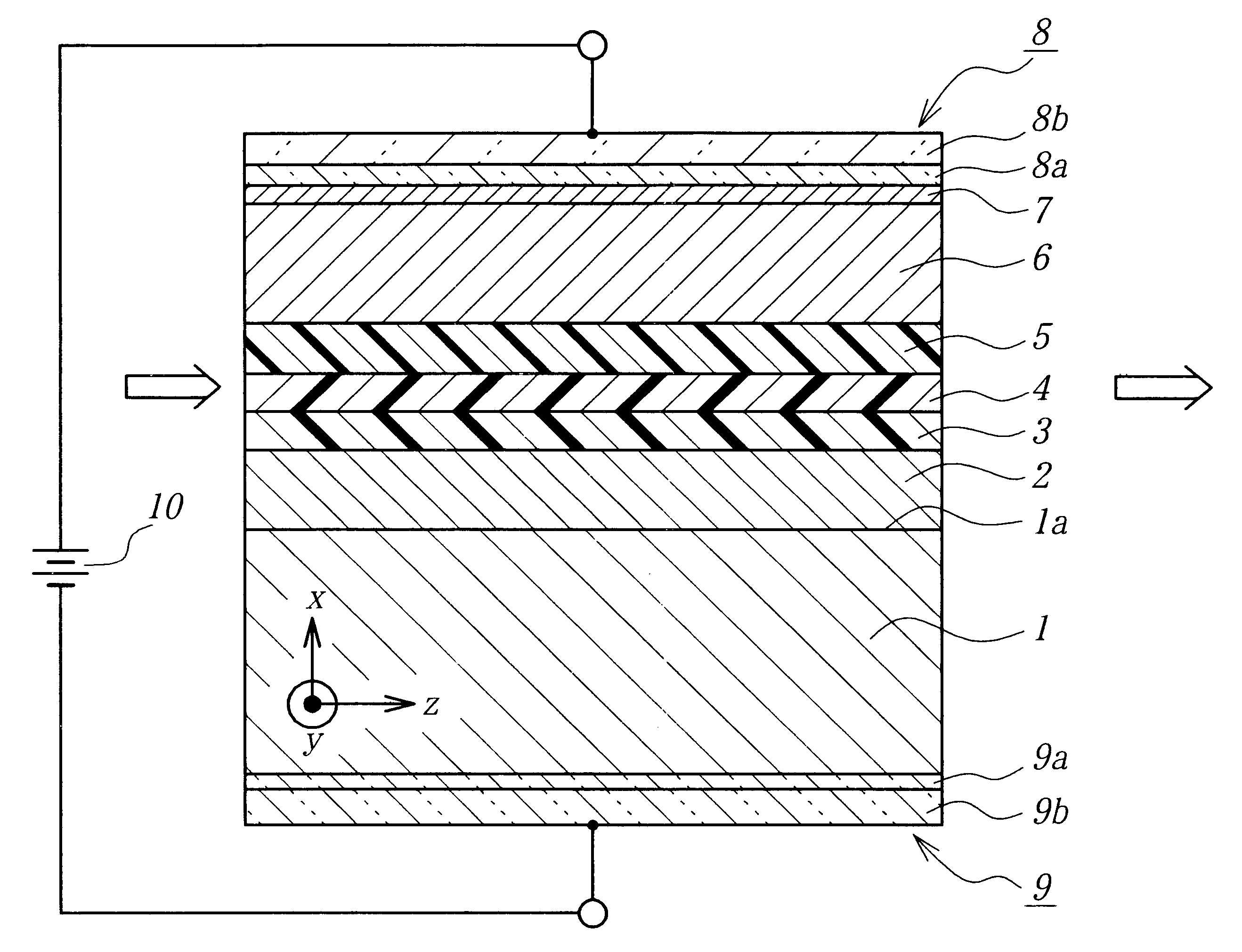
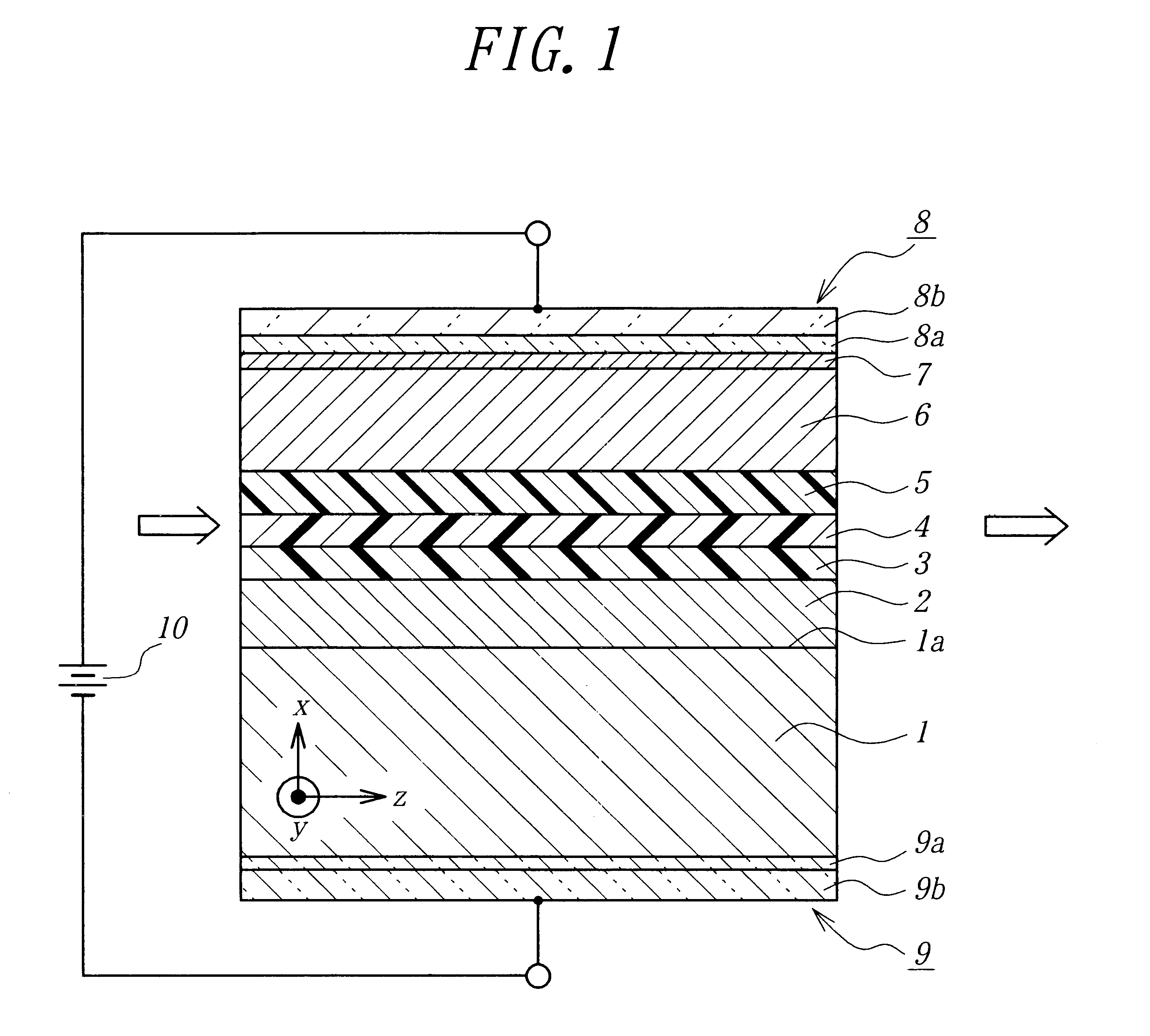
Now to the drawings, there is shown an embodiment of an optical waveguide isolator according to the present invention. FIG. 1 is a diagrammatic cross-sectional view showing the constitution of one embodiment of the optical waveguide isolator according to the present invention. This embodiment explains the optical waveguide isolator having a semiconductor optical amplifier structure for amplifying and emanating incident light. In FIG. 1, assuming that the light wave is propagated to a z direction, and a semiconductor layer structure is formed along an x direction. Substrate 1 of InP of n type is prepared, and the semi-conductor layer structure is formed on a layer forming surface 1a of the substrate.

Substrate 1 has the thickness of 100 .mu.m, and the high impurity concentration is assumed to be 1.times.1018 atoms / cm.sup.3 for example. For example, the sulfur can be used as impurities of n type.

First cladding layer 2 of n type InP is deposited on the substrate 1 of InP. First cladding...


PUM

PropertyMeasurementUnit
lengthaaaaaaaaaa
thicknessaaaaaaaaaa
thicknessaaaaaaaaaa

Abstract

An optical waveguide isolator for use in an optical communication system is disclosed. The optical waveguide isolator comprises a semiconductive light amplifier structure including a semiconductor substrate of first conductivity type having a surface of a layer to be formed thereon, a first cladding layer of first conductivity type formed on the substrate, an active layer formed on the first cladding layer, a second cladding layer of the second conductivity type opposite to first conductivity type, formed on active layer, a first electrode formed on the surface of the semiconductor substrate opposite to the surface to be formed as a layer, and a second electrode formed on the second cladding layer; the first and the second cladding layers and the active layer form an optical waveguide in which the light wave propagates. The semiconductive light amplifier structure further comprises a light absorptive magnetic material layer having light absorption function for the light wave propagating through the optical waveguide. The magnetic material layer is magnetized so as to have the magnetic-field component in the direction which corresponds to the direction where a magnetic vector of the light wave vibrates, the waveguide structure body has a nonreciprocity optical characteristic that effective refractive index changes into the light wave to which the optical waveguide is propagated according to the magnet-optical effect of the light absorptive magnetic material layer according to the direction of propagation, by the effective refractive index change in the nonreciprocity, the attenuation of the first light wave that the optical waveguide is propagated in the first direction caused when the said waveguide is propagated, becomes small more than the attenuation of the second light wave propagated in the second direction opposite to the first direction caused when the said waveguide is propagated.

Description

1. Field of the InventionThe present invention relates to an optical isolator, especially an optical wave guide capable of being integrated on a substrate together with a semiconductor laser and an optical wave guide.2. Related Art StatementIn the optical communication system, an optical isolator is used to prevent reflected light and scattered light in the end face of the optical fiber from returning to a light source side. An optical isolator using a rotation of polarization plane according to the optical-magnet material, has been put to practical use as an optical isolator now. For example, the optical isolator of Farady rotation type is constituted by a polarizer, a Faraday rotator of optically transparent material and an analyzer, so that polarized components corresponding to the plane of polarization of polarizer out of advanced circular polarization of light to the forward direction, pass through the polarizer, the plane of polarization rotates by Faraday rotator by 45.degree...

Claims


Application Information

Patent Timeline
Patent Type & Authority Patents(United States)
IPC IPC(8): G02F1/095G02F1/01G02B27/28G02B6/12H01S5/00H01S5/026H01S5/50
CPCG02F1/0955H01S5/50H01S5/0064H01S5/026
Inventor NAKANO, YOSHIAKITAKENAKA, MITSURU
Owner THE UNIV OF TOKYO
Why Eureka
Try Eureka