
Etchant for copper or copper alloy, liquid for etching pretreatment, and etching method

a technology of liquid etching and copper or copper alloy, which is applied in the direction of printed circuit manufacturing, surface treatment compositions, chemistry apparatus and processes, etc., can solve the problems of reducing the top or bottom width of the conductor pattern, unable to keep the area necessary for mounting parts, and difficult to produce printed wiring boards having a high circuit density, etc., to achieve enhanced effect on the improvement of product yield and high degr

Inactive Publication Date: 2011-03-03
MITSUBISHI PAPER MILLS LTD
View PDF7 Cites 8 Cited by
  • Summary
  • Abstract
  • Description
  • Claims
  • Application Information

AI Technical Summary

Benefits of technology

[0022]According to the etchant for copper or copper alloy in this invention, which contains water as a main component and comprises (1) 1 to 20 mass % of iron (III) chloride and (2) 5 to 100 mass %, based on the iron chloride, of oxalic acid, and the etching method using the above etchant, copper or copper alloy can be etched without causing any heavy side etch. Further, according to the liquid for etching pretreatment for copper or copper alloy in this invention, which contains water as a main component and comprises at least one component selected from a component that dissolves copper or copper alloy, and an acid, and the etching method which implements pretreatment with the above liquid for etching pretreatment, there can be prevented a defect (to be referred to as “remainder defect” hereinafter) in which copper or copper alloy that is a material to be etched remains in the form of a granule or a streak on a resist-pattern-free portion, whereby the yield of products that are produced from them can be improved.
[0023]When the acid contained in the liquid for etching pretreatment in this invention is a monovalent acid, the remainder defect can be suppressed to a high degree. When the acid contained in the liquid for etching pretreatment in this invention is an aliphatic hydroxycarboxylic acid, the remainder defect can be also suppressed to a high degree. When the liquid for etching pretreatment in this invention contains a component for dissolving copper or copper alloy and has a pH of 3 or less, the remainder defect can be also suppressed to a high degree. When the liquid for etching pretreatment in this invention contains a surfactant, the effect on the improvement of the product yield can be enhanced.
[0024]In the liquid for etching pretreatment in this invention, the component that dissolves copper or copper alloy is iron (III) chloride or copper (II) chloride, so that the yield can be improved without making a side etch bigger or making production steps complicated.
[0025]After the pretreatment, the material to be etched is washed and then etched, so that the yield can be improved without making a side etch bigger.
[0026]That is, by the etchant for copper or copper alloy, the liquid for etching pretreatment for copper or copper alloy and the method of etching copper or copper alloy in this invention, the production of printed wiring boards having high circuit densities by a subtractive method, which has been conventionally difficult, can be accomplished. Moreover, the etchant of this invention does not generate toxic gases such as hydrogen sulfide, and contains only those components whose waste disposals have been entrenched, so that the disposal thereof after use can be easily and completely done and that it is easy to get around the problems relating to industrial hygiene, pollution prevention and environmental protection. Further, according to a preferred embodiment of this invention, printed wiring boards having high circuit densities can be produced with excellent yields.BRIEF EXPLANATION OF DRAWINGS
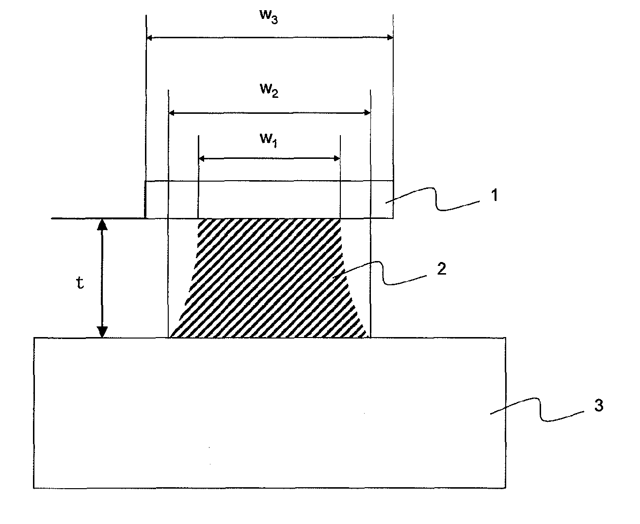
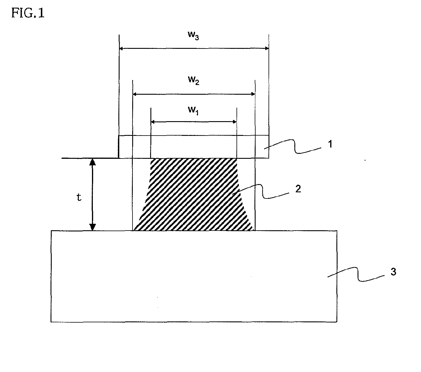
[0027]FIG. 1 is a schematic cross-sectional view of a conductor pattern obtained by an etching method.

Problems solved by technology

When the side etch takes place, the top width or bottom width of the conductor pattern is decreased, and there is caused a problem that an area necessary for mounting parts cannot be kept, so that it has been difficult to produce a printed wiring board having a high circuit density by the subtractive method.
However, the additive method essentially has a problem that its cost becomes very high, since it includes complicated steps and is carried out through a plating step that requires a long time period.
When the top width w1 or bottom width w2 is too small, no sufficient electric characteristic can be maintained.
Further, when the top width w1 is too small, it is difficult to mount a component on its surface.
When the top width w1 of a conductor pattern is extremely smaller than the line width w3 of a resist pattern, there is also caused a problem that the resist pattern 1 peels off the copper foil 2 during etching to break the conductor pattern.
Further, when the bottom width w2 is too small, there is caused a problem that a conductor peels off the substrate 3 to break the conductor pattern.
In this technique, not only the capability of suppressing a side etch is insufficient for producing very high-density boards that are demanded in recent years, but also it uses thiourea that is suspected of being carcinogenic, or further it has a serious problem from the viewpoint of industrial hygiene and pollution control that the etchant generates hydrogen sulfide gas that is a toxic and malodorant substance when the etchant is stored or used.
However, not only this technique is also insufficient in capability of suppressing a side etch, but it also has a serious problem from the viewpoint of environmental protection that it uses an azole compound that generally has low biodegradability.
However, this etchant is not intended for precision processing that has been demanded in recent years.
When it is used for producing a printed wiring board having a fine pitch as described above, the etching speed rapidly increases after the etching proceeds to a certain degree, and the line width rapidly decreases, so that it has been practically impossible to control the etching.

Method used


Image

  • Etchant for copper or copper alloy, liquid for etching pretreatment, and etching method
  • Etchant for copper or copper alloy, liquid for etching pretreatment, and etching method
  • Etchant for copper or copper alloy, liquid for etching pretreatment, and etching method

Examples


example 1

Preparation of Etchant

[0062]Water was added to 27 g (10 g as an anhydride) of a commercially available 40° Be iron (III) chloride aqueous solution (concentration 37 mass %) and 0.70 g (0.50 g as an anhydride) of oxalic acid dihydrate up to a total amount of 1 kg, to prepare an etchant containing 1.0 mass % of iron (III) chloride and 0.050 mass % of oxalic acid.

[0063]1 to be Etched>

[0064]A positive liquid resist was applied to the surface of a copper-clad laminate obtained by bonding a 1.6 mm thick glass epoxy substrate (FR-4 standard) and a 12 μm thick electro-deposited copper foil to each other, such that a layer on the surface had a dry thickness of 6 μm, followed by drying. Then, an exposure through a pattern having line / space widths of 15 μm / 15 μm for evaluation was carried out, and then a resist pattern was formed by development and washing with water to make a material 1 to be etched.

[0065]

[0066]The above etchant adjusted to 30° C. was ejected to the material 1 to be etched by...

examples 2-8

[0067]Etchants containing iron (III) chloride and oxalic acid having concentrations shown in Tables 1 and 2 were prepared in the same manner as in Example 1, and the same materials to be etched as that of Example 1 were spray-etched under ejection conditions as specified. (1) Ejection time periods X (second) it took to reach w2=w3 (15 μm), (2) w1 and w2 when the ejection time periods were set to 1.2 times as long as X and (3) w1 and w2 when the ejection time periods were set to 2.0 times as long as X were measured. Tables 1 and 2 show the results.

example 9

Preparation of Etchant

[0071]Water was added to 13.5 kg (5.00 kg as an anhydride) of a commercially available 40° Be iron (III) chloride aqueous solution (concentration 37 mass %) and 1.40 kg (1.00 kg as an anhydride) of oxalic acid dihydrate up to a total amount of 100 kg, to prepare 100 kg of an etchant containing 5.0 mass % of iron (III) chloride and 1.0 mass % of oxalic acid.

[0072]

[0073]Grams of sulfuric acid (concentration 98 mass %) was added to 980 g of water, and they were fully mixed to prepare a pretreatment liquid having a concentration of 2.0 mass %.

[0074]2 to be Etched>

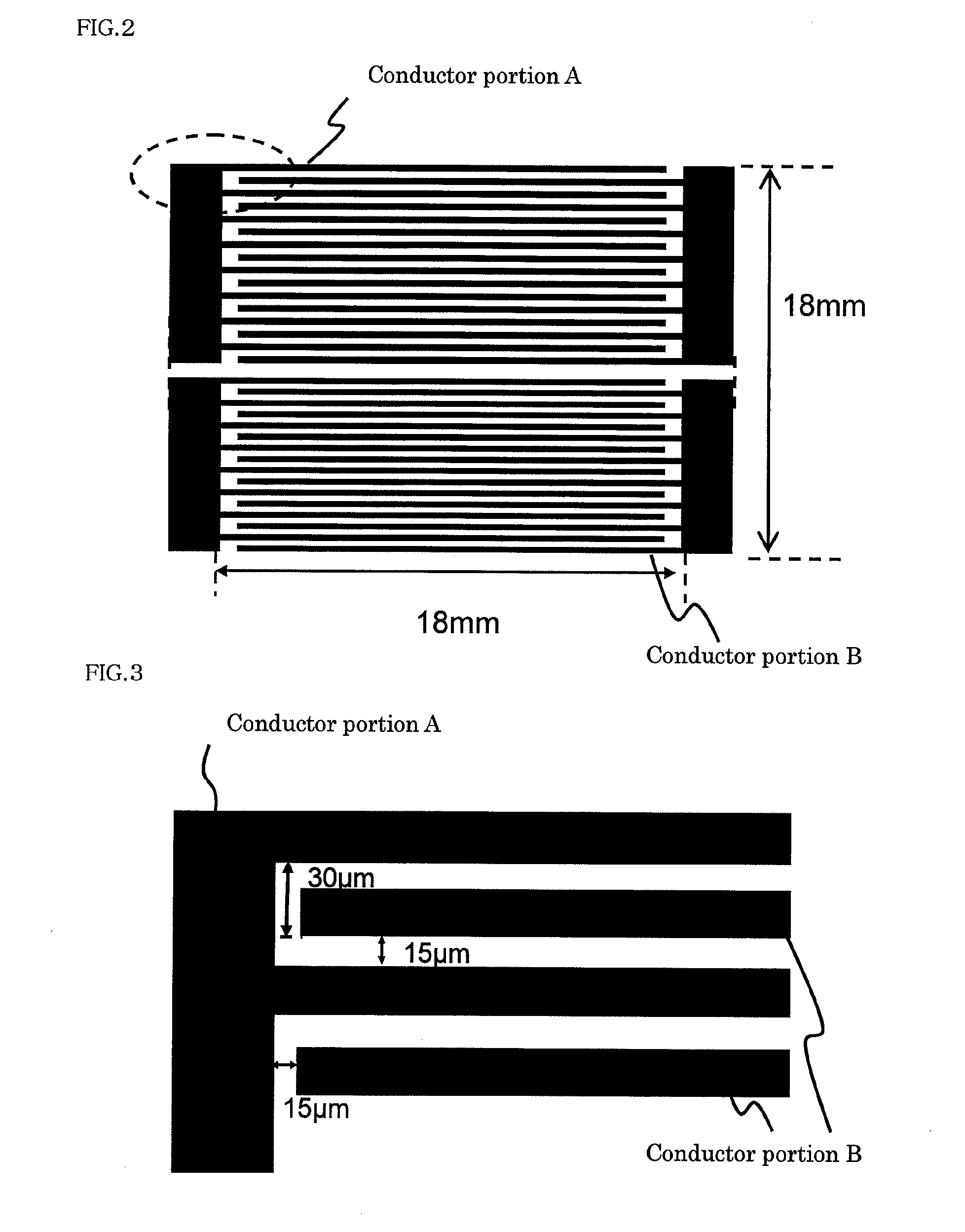
[0075]A positive liquid resist was applied to the surface of a copper-clad laminate obtained by bonding a 40 μm thick polyimide insulating material and a 9 μm thick electro-deposited copper foil, such that a layer on the surface had a dry thickness of 6 μm, followed by drying. A resist pattern of 100 blocks having a comb type wiring shown in FIG. 2 each was formed thereon to make a material 2 to be etched....


PUM

PropertyMeasurementUnit
pHaaaaaaaaaa
thicknessaaaaaaaaaa
thicknessaaaaaaaaaa

Abstract

An etchant for copper or copper alloy, which contains water as a main component and comprises (1) 1 to 20 mass % of iron (III) chloride and (2) 5 to 100 mass %, based on the iron chloride, of oxalic acid, and an etching method using the above etchant are provided, and the etching method includes pretreatment to be carried out with an aqueous solution containing at least one component selected from a component that dissolves copper or copper alloy and an acid, whereby well yields can be materialized.

Description

TECHNICAL FIELD[0001]This invention relates to an etchant for copper or copper alloy suitable for producing high-density printed wiring boards, a liquid for etching pretreatment for copper or copper alloy, and a method of etching copper or copper alloy with the above etchant or liquid for etching pretreatment.BACKGROUND ART[0002]In recent years, the downsizing and functional enhancement of electronic instruments have rapidly progressed, and as regards printed wiring boards to be housed in these instruments, those which have high circuit densities are strongly required.[0003]As a method for producing printed wiring boards, there is widely employed a so-called subtractive method in which a resist pattern is formed on a substrate to which a copper foil has been beforehand bonded, by the method of screen printing, photolithography, etc., and copper foil in an unnecessary portion is removed with an etchant such as an iron (III) chloride aqueous solution, etc., to form a conductor pattern...

Claims


Application Information

Patent Timeline
Patent Type & Authority Applications(United States)
IPC IPC(8): C23F1/18C09K13/00C23F1/00
CPCC23F1/18H05K2203/1476H05K2203/0392H05K3/067
Inventor KATO, MAKOTOTOYODA, YUJINAKAGAWA, KUNIHIROISHIDA, MARIKOKANEDA, YASUO
Owner MITSUBISHI PAPER MILLS LTD
Learn More