Dual damascene process for carbon-based low-K materials

a technology of carbon-based low-k materials and damascene, which is applied in the direction of basic electric elements, semiconductor/solid-state device manufacturing, electric devices, etc., can solve the problems of shortening the device life and reliability, and not enough etch selectivity between the organic low-k material and the bar

Inactive Publication Date: 2001-04-03
TAIWAN SEMICON MFG CO LTD
View PDF11 Cites 88 Cited by
  • Summary
  • Abstract
  • Description
  • Claims
  • Application Information

AI Technical Summary

Problems solved by technology

Conductors having high resistivity create conduction paths with high impedence and large propagation delays, resulting in shorter device life and reliability problems.
High-K dielectrics have cause high capacitance resulting in shorter device life and reliability problems.
However, there are fabrication problems associated with a copper dual damascene process with an organic, low-K dielectric material, due to the lack of etch selectivity between the organic, low-K dielectric material and bottom anti-reflective coating (barc), and due to the undesireability of using a high-K etch stop layer.
However, for dielectric layers composed of organic, low-K materials, there is not sufficient etch selectivity between the organic low-K material and the barc.
If barc material remains it can not easil...

Method used


Image

  • Dual damascene process for carbon-based low-K materials
  • Dual damascene process for carbon-based low-K materials
  • Dual damascene process for carbon-based low-K materials

Examples


Embodiment Construction

-FIGS. 4, 5A, 5B, 6A, 6B & 7

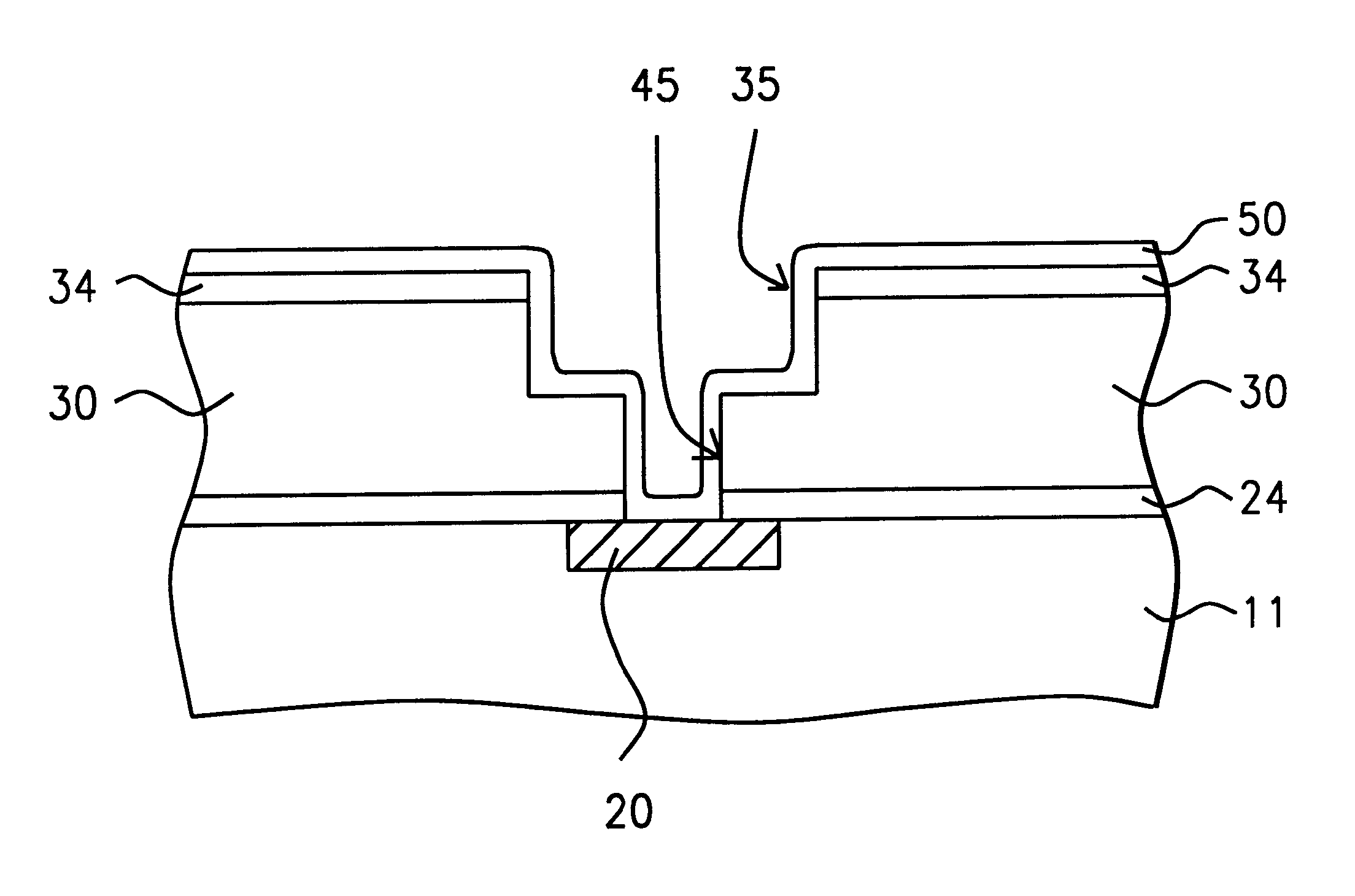
The preferred embodiment of the present invention provides a method for forming a dual damascene structure in a carbon-based, low-K dielectric layer, without causing increased capacitance or damaging the dielectric layer.

Referring to FIG. 4, the preferred embodiment of the present invention begins by providing a semiconductor structure (11). Semiconductor structure (11) should be understood to possibly comprise a substrate comprised of semiconducting material such as silicon or germanium, or a silicon on insulator structure (SOI) as is known in the art. Semiconductor structure (11) should be understood to possibly further include one or more conductive layer (such as metal or silicon) and / or insulating layers, and one or more active or passive devices formed in or over the substrate or the like.

Still referring to FIG. 4, a first metal pattern (20) is formed on the semiconductor structure (11). A first barrier layer (24) is formed on the first metal patter...


PUM


Abstract

A method for forming a dual damascene structure in a carbon-based, low-K material. The process begins by providing a semiconductor structure having a first metal pattern thereover, wherein the first metal pattern has a first barrier layer thereon. An organic dielectric layer is formed on the first barrier layer, and a hard mask layer is formed on the dielectric layer. The hard mask layer and the dielectric layer are patterned to form a trench. A second barrier layer is formed over the hard mask layer and on the bottom and sidewalls of the trench. A barc layer is formed over the second barrier layer, thereby filling the trench. The barc layer, the second barrier layer, and the dielectric layer are patterned to form a via opening, preferably using a photoresist mask. The barc layer is patterned without faceting the edges of the via opening due to the second barrier layer. The barc layer and the etch mask are removed by the dielectric layer etch. The first barrier layer and the second barrier layer are removed. A third barrier layer is formed on the bottom and sidewalls of the trench, on the sidewalls of the via opening, and on the first metal pattern through the via opening. The trench and the via opening are filled with metal to form a damascene structure.

Description

DESCRIPTION OF THE PRIOR ARTIn current IC fabrication, connections between metal levels, such as copper, which are separated by dielectric interlevels, are typically formed with a damascene method of via formation between metal levels. The first metal pattern is first completely covered with dielectric, such as silicon dioxide. A trench is patterned into the dielectric layer. A via is patterned from the trench, through the dielectric layer, to the first metal pattern. A metal film, such as copper, is then used to fill the via and the trench. A layer consisting of dielectric with a metal via through it now overlies the first metal pattern. The excess metal can be removed using a CMP process, as is well known in the art. The result is an "inlaid", or damascene metal structure.As devices continue to be smaller, less expensive, and more powerful, smaller geometries and denser packaging are required for integrated circuits. Conductors having high resistivity create conduction paths with ...

Claims


Application Information

Patent Timeline
IPC IPC(8): H01L21/768H01L21/70
CPCH01L21/76808
Inventor CHEN, CHAO-CHENGLUI, MING-HUEILIU, JEN-CHENGCHAO, LI-CHIHTSAI, CHIA-SHIUNG
Owner TAIWAN SEMICON MFG CO LTD
Why Eureka
Try Eureka