Group III nitride field emitters

a field emitter and nitride technology, applied in the manufacture of electrode systems, electric discharge tubes/lamps, discharge tubes, etc., can solve the problems of high vacuum required during operation, low life of emission tip, and increased fabrication costs

Inactive Publication Date: 2001-04-17
HOUSTON UNIV OF
View PDF4 Cites 31 Cited by
  • Summary
  • Abstract
  • Description
  • Claims
  • Application Information

AI Technical Summary

Problems solved by technology

They are difficult to manufacture, variation of emission current can be significant over large areas such as those required for flat displays, the lifetime of the emission tip is low due to the large current flow through a very small area and the high vacuum required during operation can be expensive.
Diamond surfaces are very sensitive to oxygen, however, and must be packaged under a vacuum, which increases fabrication cost.
This limits the use of diamond for such applications as ion source cathodes or micro electromechanical systems (MEMS), for example, where oxygen is often a process envi...

Method used


Image

  • Group III nitride field emitters
  • Group III nitride field emitters
  • Group III nitride field emitters

Examples


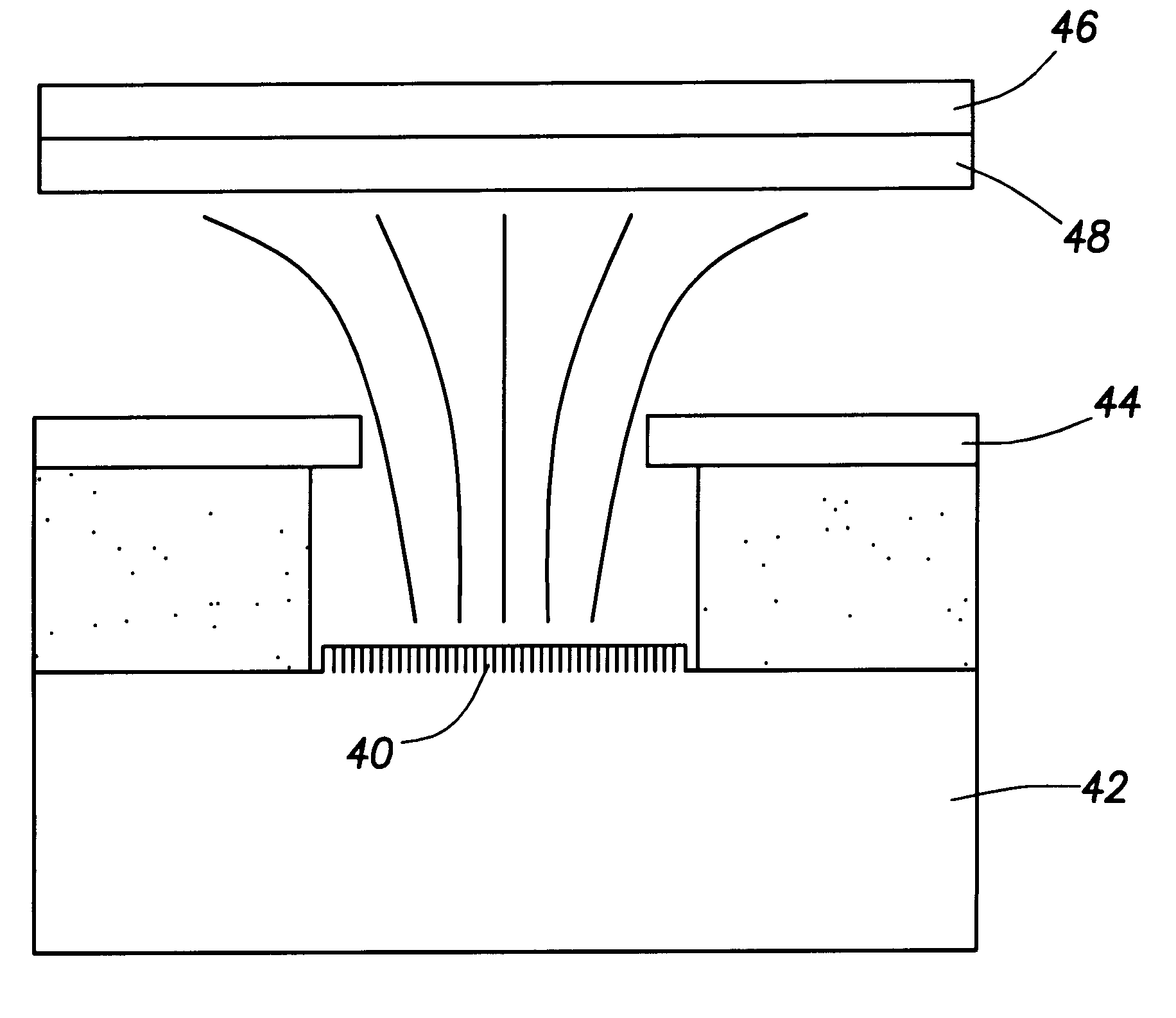
Embodiment Construction

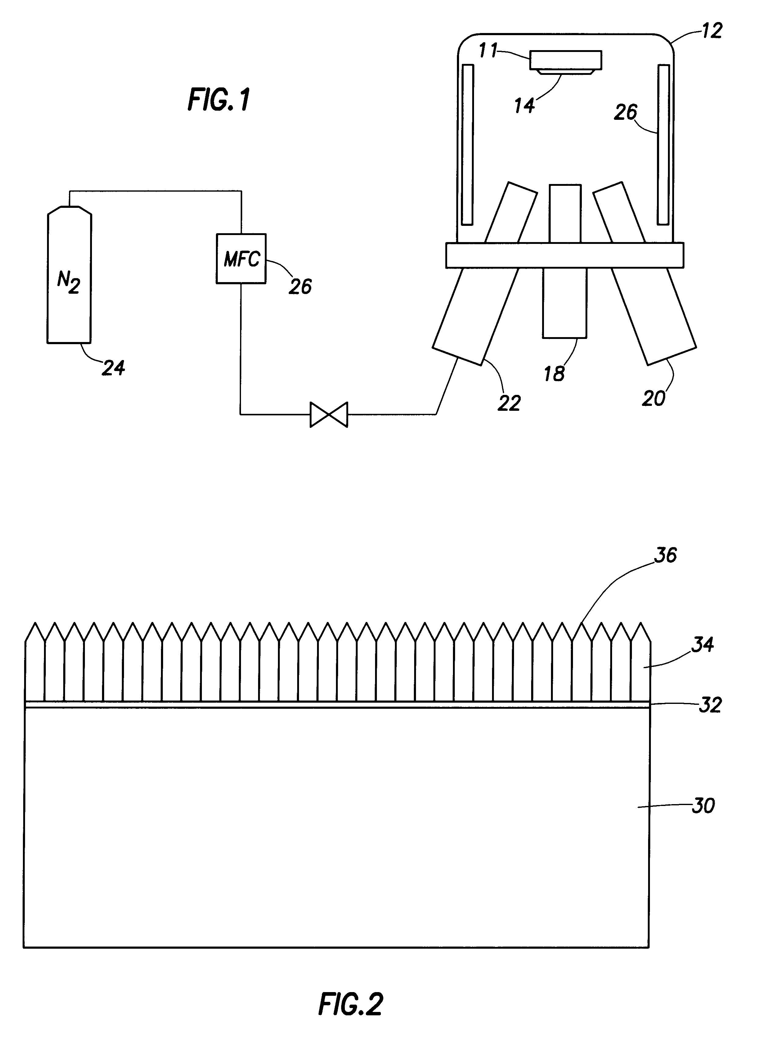
a. Substrate Preparation

Commercial 500 .mu.m thick, n-type low-resistivity Si wafers with a (111) surface orientation were etched first in HF (10% water solution) for 1 minute. The etching process was terminated by washing the wafer in methanol without contact with air. In addition, the wafer was cleaned in an ultrasound bath with methanol twice for 10 minutes each. Care was taken to avoid contact of the substrate with air. The wafer was transferred to the loading area immersed in methanol. Just before loading, the wafer was dried by nitrogen flow. The wafer was then loaded immediately.

b. Loading of the Substrate Into the Growth Chamber and Annealing

Immediately after the Si wafer was dried by nitrogen, it was transferred to the loading chamber and on to a molybdenum sample carrier and placed on the transfer rod. (It is preferable to carry out all procedures in a nitrogen ambient in order to avoid any contact between the etched Si wafer and air.) The loading chamber was pumped down b...


PUM


Abstract

Field emitter as a source of electrons and method for making are provided. The emitter is formed by growth of a nitride compound of a group III element or alloys of group III elements on a substrate having a lattice mismatch with the thin film. The lattice mismatch causes columnar growth in the film. The micro columns have tips, thus forming an array of crystalline microtips of the low work function nitride material. The nitride compound is doped during growth. Gallium nitride grown on (111) silicon and doped with silicon produces a surface having low threshold electric field for emission and high current per unit area.

Description

1. Field of the InventionThis invention relates to field emission cathodes and method for making. More particularly, group III nitride thin films grown on silicon or other substrates to form a high density of field emission micro-tips and method for making are provided.2. Description of Related ArtField emission of electrons from solid surfaces can provide a cold cathode for use in displays and other devices of vacuum microelectronics. In field emission, flow of electrons from the surface of a solid material into a surrounding vacuum occurs under the influence of an applied electric field. In order to be emitted, an electron must propagate through a potential barrier between the surface and the vacuum. Quantum mechanical tunneling makes such propagation possible.The potential barrier that the electron must overcome depends on the material's "electron affinity," which is a constant for each given surface and is different for different materials. Most materials have large positive ele...

Claims


Application Information

Patent Timeline
IPC IPC(8): H01J1/304H01J1/30H01J9/02
CPCH01J1/304H01J9/025
Inventor BERISHEV, IGORBENSAOULA, ABDELHAK
Owner HOUSTON UNIV OF
Why Eureka
Try Eureka