Process for filling apertures in a circuit board or chip carrier
a technology of circuit board and chip carrier, which is applied in the field of filling apertures in can solve the problems of achieve the effect of not adversely affecting the dimensional stability of the printed circuit board or chip carrier, and avoiding dimensional changes
- Summary
- Abstract
- Description
- Claims
- Application Information
AI Technical Summary
Benefits of technology
Problems solved by technology
Method used
Image
Examples
second embodiment
In the case of the first described process whereby the exposure is restricted to only the depth of the thickness on the substrate but leaves unexposed material located in the apertures, the development step results in a planarized surface suitable for subsequent circuitization. On the other hand, described above whereby selective exposure is conducted, there will remain a raised portion within the vicinity of apertures, commonly referred to as a "nub" which must be removed to achieve a planarized surface. This can be readily achieved by chemical-mechanical polishing. In any event, the final structure will be a planarized surface that is capable of being circuitized.
The following non-limiting examples are presented to further illustrate the present invention.
example 1
A mixture consisting of 8 gr of an epoxide cresol novolak, Araldite ECN-1280, 2 gr of talc, 0.08 g of ethyl violet, 0.24 g of Irgacure 261, 0.1 g of 2-methylimidazole, 5 gr of methyl ethyl ketone and 5 gr of propylene glycol monomethyl ether acetate is applied onto a 3 mil mylar film by means of a 20 wire doctor-blade. The film is then dried at 100.degree. C. for about 10 minutes. The coated film is subsequently laminated onto a circuit board with the light sensitive material facing and contacting the circuit board. The dielectric material under pressure flows into the vias or apertures while the temperature is raised from room temperature to 150.degree. C. After lamination the supporting film can be removed, the photosensitive layer is exposed to actinic radiation, baked, and subsequently developed with the unexposed areas remaining intact.
example 2
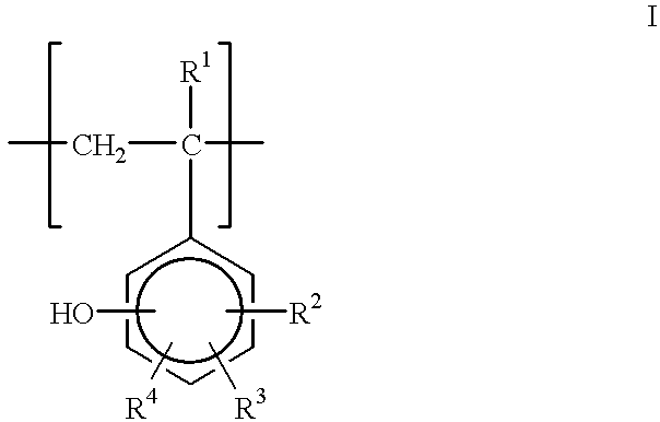
A mixture consisting of 11 gr of an epoxide bisphenol A diglycidyl ether (Epon-828), 10 gr of poly-p-vinylphenol (m.w. 1000), 0.44 g of Irgacure 261, 0.2 g of 2-methylimidazole, 5 gr of methyl ethyl ketone and 5 gr of propylene glycol monomethyl ether acetate is applied onto a 3 mil mylar film by means of a 20 wire doctor-blade. The film is then dried at 100.degree. C. for about 10 minutes. The coated film is subsequently laminated onto a circuit board with the light sensitive material facing and contacting the circuit board. The dielectric material under pressure flows into the vias or apertures while the temperature is raised from room temperature to 150.degree. C. After lamination the supporting film can be removed, the photosensitive layer is exposed to actinic radiation, baked, and subsequently developed with the unexposed areas remaining intact. The developer solution in this example is made of 37.35 g of sodium metasilicate pentahydrate and 2 gr of 2-ethoxyethanol in 1 liter ...
PUM
 Abstract
Description
Claims
Application Information
