Method for forming a square oxide structure or a square floating gate structure without rounding effect

Inactive Publication Date: 2001-06-12
TAIWAN SEMICON MFG CO LTD
View PDF6 Cites 9 Cited by
  • Summary
  • Abstract
  • Description
  • Claims
  • Application Information

AI Technical Summary

Benefits of technology

It is yet another object of the present invention to provide a method for forming square floating gates in a split-gate cell with a reduced gap width therebetween.
The present invention provides considerable improvement over the prior art. The key advantage of the present invention is that the two separate, perpendicular masks used to form a square opening reduce the rounding effect that occurs due to the photolithography process. The present invention provides square structures without rounded corners, thereby inproving device performance, especially when mismatch occurs.
Also, because the polyoxide hard mask formed in accordance with the present invention grows in width by the length of the bird's beaks which form during oxidation, the gap can be reduced by two times the length of the birds beak.

Problems solved by technology

However, due to limitations of the photolithography process, the corners of square openings in the photosensitive mask become rounded.
As device dimensions continue to shrink, this rounding effect at the corners of square structures can have a detrimental effect on device performance.
This detrimental effect can be worse when mis-alignment between photolithography masks occurs.
Another problem which occurs as packing density increases, is that the gap between floating gates in a split cell memory device is limited by the photolithography process.

Method used


Image

  • Method for forming a square oxide structure or a square floating gate structure without rounding effect
  • Method for forming a square oxide structure or a square floating gate structure without rounding effect
  • Method for forming a square oxide structure or a square floating gate structure without rounding effect

Examples


second preferred embodiment

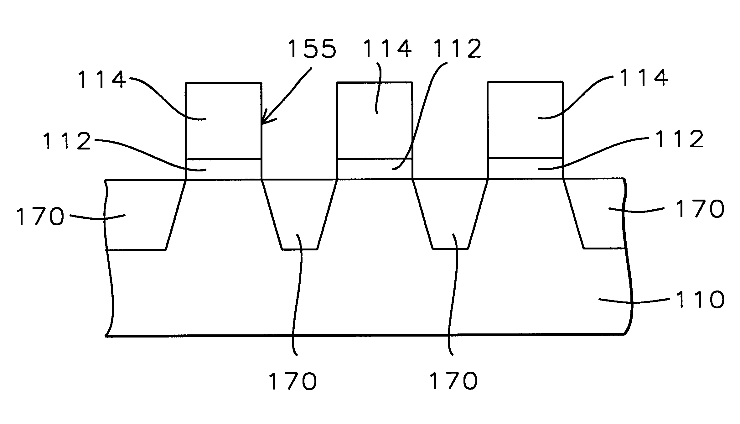
Referring to FIG. 5, the second preferred embodiment of the present invention begins by providing a semiconductor structure (210). Semiconductor structure is to be understood to comprise a substrate such as a silicon wafer or a silicon on insulator substrate. Semiconductor structure is to be understood to possibly further comprise one or more conductive layers (e.g. polysilicon, metal, etc) and / or dielectric layers (e.g. inter poly oxide layer, intermetal dielectric layer, etc) and active and / or passive devices formed in or over the substrate. In the second preferred embodiment, the semiconductor structure (210) preferably comprises a substrate composed of monocrystalline silicon.

A gate oxide layer (212) is formed on the semiconductor structure (110). The gate oxide layer (212) is preferably thermally grown to a thickness of between about 80 Angstroms and 100 Angstroms at a temperature of between about 800.degree. C. and 900.degree. C.

A polysilicon layer (214) is formed on the gate ...


PUM


Abstract

A method for forming a square oxide structure or a square floating gate without a rounding effect at its corners. A first dielectric layer is formed on a pad layer for a square oxide structure or a polysilicon layer overlying a gate oxide layer for a floating gate, and a second dielectric layer is formed on the first dielectric layer. The second dielectric layer is patterned to form parallel openings in a first direction using a first photosensitive mask. A second photosensitive mask, having a plurality of parallel openings in a second direction perpendicular to the first direction is formed over the second dielectric layer and the first dielectric layer. The first dielectric layer is etched through square openings where the openings in the second photosensitive mask and the openings in the second dielectric layer intersect, thereby forming square openings in the first dielectric layer. The second photosensitive mask and the second dielectric layer are removed. The square oxide structure is completed by etching a trench in the semiconductor structure and forming an STI or LOCOS. The square floating gate is completed by growing polysilicon oxide structures in the square openings in the first dielectric layer and removing the first dielectric layer to form a pattern of openings therebetween, and etching the polysilicon layer through the pattern of openings between the polysilicon oxide structures forming square floating gate polysilicon regions under the polysilicon oxide hard masks.

Description

1) Field of the InventionThis invention relates generally to fabrication of a semiconductor device and more particularly to a method for forming a square oxide structure or a square floating gate structure without a rounding effect at the corners of the square oxide structure or the square floating gate structure.2) Description of the Prior ArtThe use of a silicon nitride layer as an oxidation mask is well known. To form square structures, such as oxide isolation structures or floating gates in a split cell memory, a photosensitive mask is formed with square openings, and the silicon nitride layer is etched through these openings.However, due to limitations of the photolithography process, the corners of square openings in the photosensitive mask become rounded. This rounding of the corners of a square opening in a photosensitive mask is known as a rounding effect. As device dimensions continue to shrink, this rounding effect at the corners of square structures can have a detrimenta...

Claims


Application Information

Patent Timeline
IPC IPC(8): H01L21/02H01L21/70H01L21/28H01L27/115H01L21/311H01L21/8238H01L21/32H01L21/8247
CPCH01L21/28114H01L21/28123H01L21/31144H01L21/32H01L21/823842H01L27/115H01L27/11521H10B69/00H10B41/30
Inventor SUNG, HUNG-CHENGKUO, DI-SONHSIEH, CHIA-TA
Owner TAIWAN SEMICON MFG CO LTD
Why Eureka
Try Eureka