Circuitry interconnection method

a technology of interconnection and circuit, applied in the direction of printed circuit aspects, instruments, chemistry apparatus and processes, etc., can solve the problems of less than desirable adhesion degree and less than desired conductivity in the interconnection, and achieve the effect of enhancing the adhesion of bumps

Inactive Publication Date: 2001-06-26
ROUND ROCK RES LLC
View PDF27 Cites 13 Cited by
  • Summary
  • Abstract
  • Description
  • Claims
  • Application Information

AI Technical Summary

Benefits of technology

The invention comprises circuitry interconnection methods. In one implementation, electrically conductive polymer bumps are formed in electrical connection with circuitry supported by a first substrate. The polymer bumps are bonded with a conductive adhesive to circuitry supported by a second substrate, with the conductive adhesive being in electrical connection with the circuitry supported by the second substrate. Prior to said bonding, an effective amount of ultraviolet radiation is impinged onto the polymer bumps to enhance adhesion of the bumps with the conductive adhesive and electrical conduction between the circuitry of the first substrate and the circuitry of the second substrate.

Problems solved by technology

In certain instances, the degree of adhesion achieved in the prior art is less than desirable.
Such can accordingly result in less than desired conductivity in the interconnect between the chip and conductive traces of the polymer sheet.

Method used


Image

  • Circuitry interconnection method
  • Circuitry interconnection method

Examples


example 2

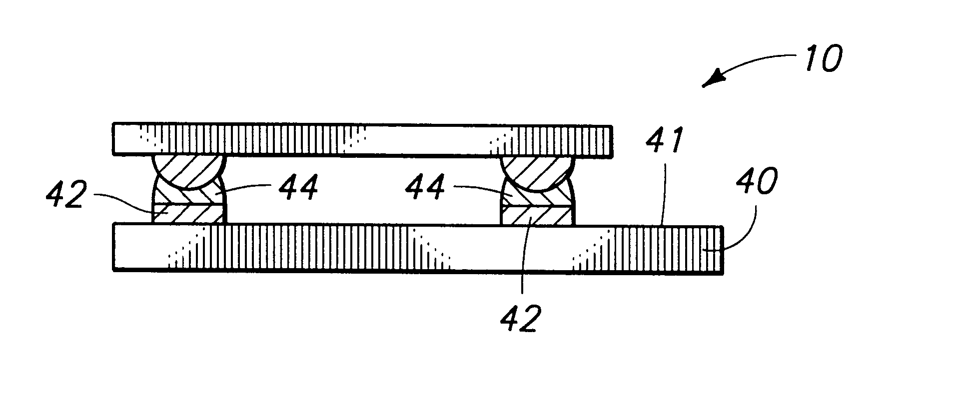
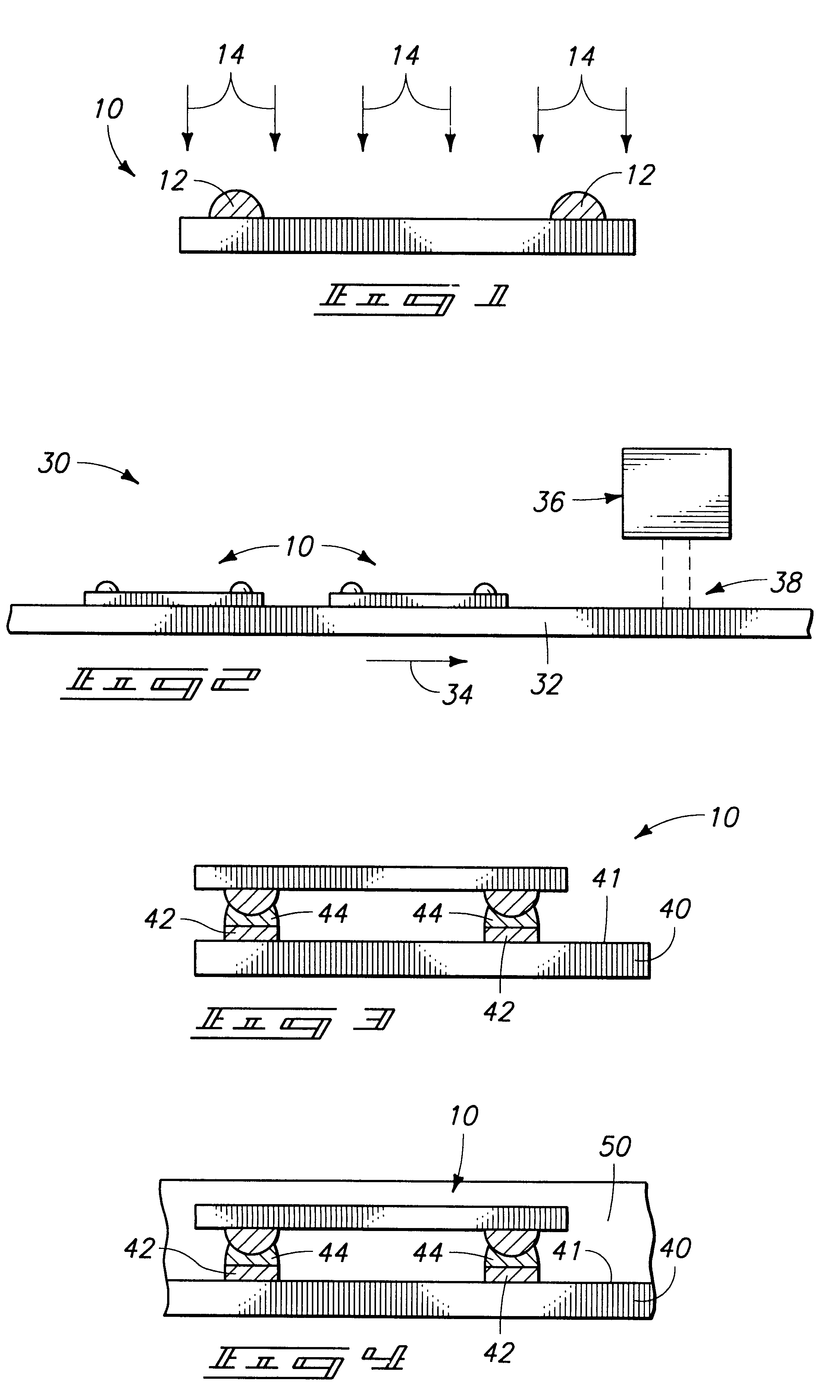
In a manner similar to Example 1, multiple substrates having exposed epoxy bumps are passed through the SPE UV ultraviolet light system. The profile within the system includes, energy of 643.60 mJ / cm.sup.2, a peak energy of 280 mW / cm.sup.2, an average energy of 90.01 mW / cm.sup.2 and a peak temperature of 116.8.degree. C. Epoxy bumps are exposed three to four times to this profile, with such providing significant increases in adhesion and conductance compared to a control substrate.

example 3

In a similar manner as described in Example 2, multiple substrates are passed through a LESCO Ultraviolet Light Curing System, available from LESCO Incorporated, Light Wave Energy Systems Company, Redondo Beach, Calif. Such system is equipped with a Fusion Systems Corporation F300-18 "D" type bulbs. The following data regarding the ultraviolet light intensity and temperature profile is used with respect to the ultraviolet light exposure per pass through the system. This profile includes ultraviolet light energy of 1.48 J / cm.sup.2 ; peak energy of 468.00 mW / cm.sup.2 ; average energy of 158.08 mW / cm.sup.2 ; and peak temperature of 72.0.degree. C. Operating at this profile, the conductive polymer bumps of the substrate passed only once through the system have considerably improved adhesion.


PUM

PropertyMeasurementUnit
wavelengthaaaaaaaaaa
ultraviolet radiation wavelengthaaaaaaaaaa

Abstract

Electrically conductive polymer bumps are formed in electrical connection with circuitry supported by a first substrate. The polymer bumps are bonded with a conductive adhesive to circuitry supported by a second substrate, with the conductive adhesive being in electrical connection with the circuitry supported by the second substrate. Prior to said bonding, an effective amount of ultraviolet radiation is impinged onto the polymer bumps to enhance adhesion of the bumps with the conductive adhesive and electrical conduction between the circuitry of the first substrate and the circuitry of the second substrate. In one implementation, ultraviolet radiation of at least 340 nm is impinged onto conductive polymer bumps prior to subsequent bonding. In one implementation, ultraviolet radiation is impinged onto conductive polymer bumps for a time period less than one minute prior to subsequent bonding. In one implementation, ultraviolet radiation is impinged onto conductive polymer bumps to provide a total ultraviolet radiation exposure of greater than about 50 mJ/cm2 prior to subsequent bonding. In one implementation, ultraviolet radiation is impinged onto conductive polymer bumps in the absence of ozone other than any produced by said ultraviolet radiation prior to subsequent bonding. In one implementation, ultraviolet radiation is impinged onto conductive polymer bumps in an atmosphere consisting essentially of ambient room air prior to subsequent bonding.

Description

This invention relates to circuitry interconnection methods.In many applications, circuitry formed on different substrates needs to be interconnected. One example would be the electrical interconnection of a monolithic integrated circuit chip with another substrate, such as a printed circuit board or a thin polyester sheet having circuit traces printed thereon. For example, U.S. Pat. No. 5,612,513; U.S. Pat. No. 5,987,739; and U.S. Pat. No. 6,031,459 disclose wireless communications devices wherein a semiconductor chip is conductively bonded to a thin polymer sheet having conductive traces including antenna fabricated thereon. Each of these documents is herein incorporated by reference.Such documents disclose electronic identification systems typically comprising two devices which are configured to communicate with one another via a wireless medium. Such communication systems can be used in various identification functions and other applications. An interrogator is configured to out...

Claims


Application Information

Patent Timeline
Patent Type & Authority Patents(United States)
IPC IPC(8): H01L21/02G06K19/077H01L23/48H01L21/60H01L23/485H05K3/32
CPCG06K19/07749H01L24/10H01L24/81H05K3/321H01L24/13G06K19/0775Y10T29/49146H01L2224/13099H01L2224/81801H01L2924/14H05K2201/0367H05K2201/10674H05K2201/10992H01L2924/01005H01L2924/01006Y10T29/4913H01L2924/00H01L2224/13
Inventor LAKE, RICKIE C.
Owner ROUND ROCK RES LLC
Why Eureka
Try Eureka