

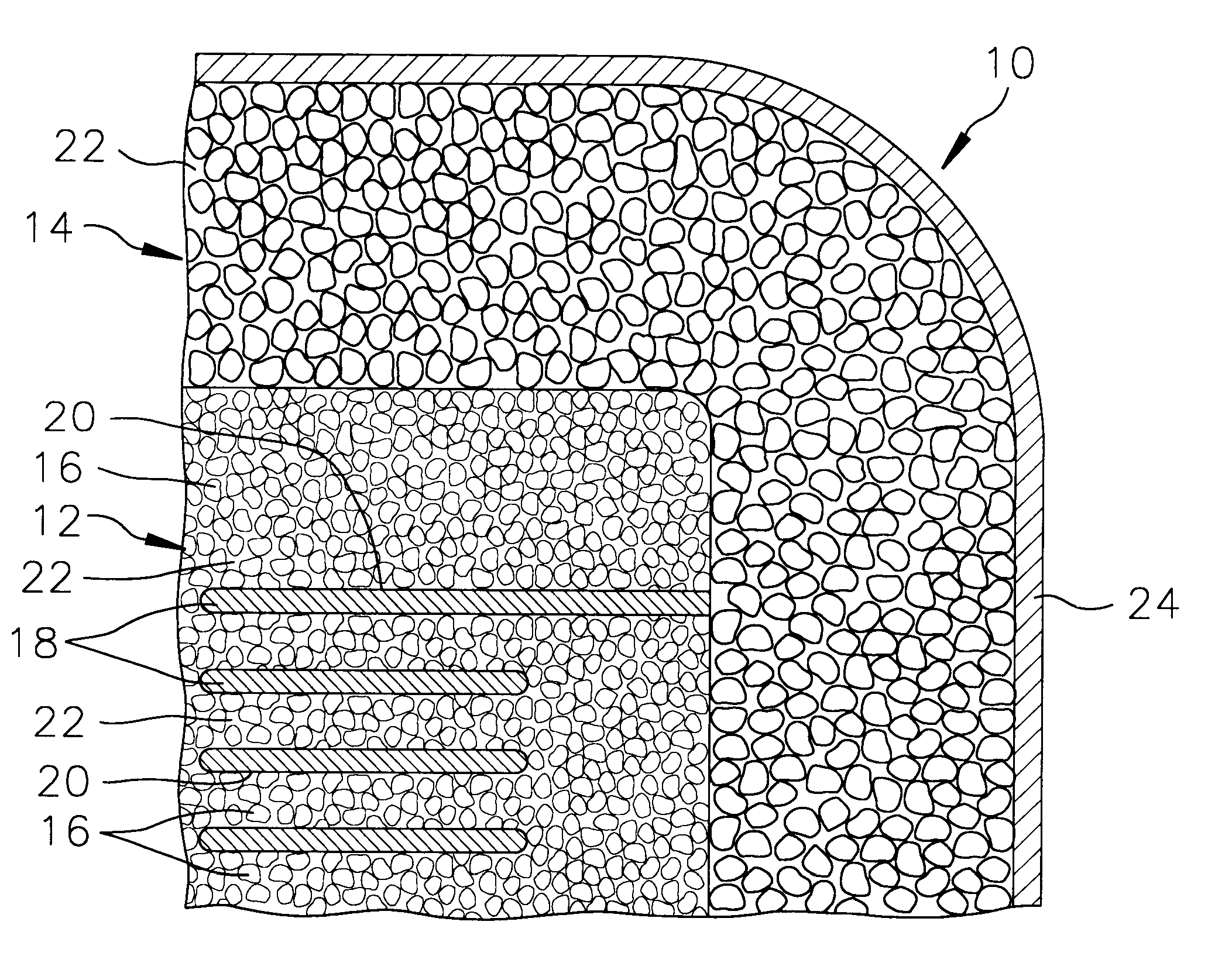
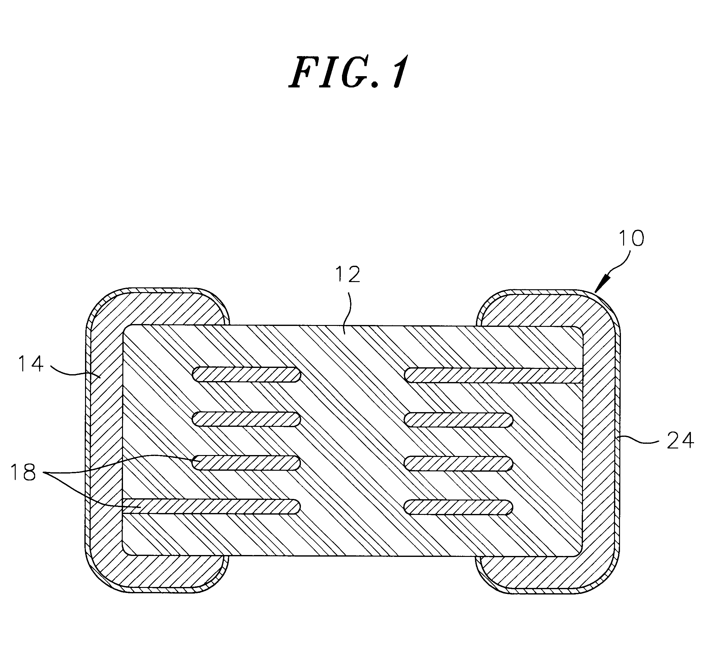
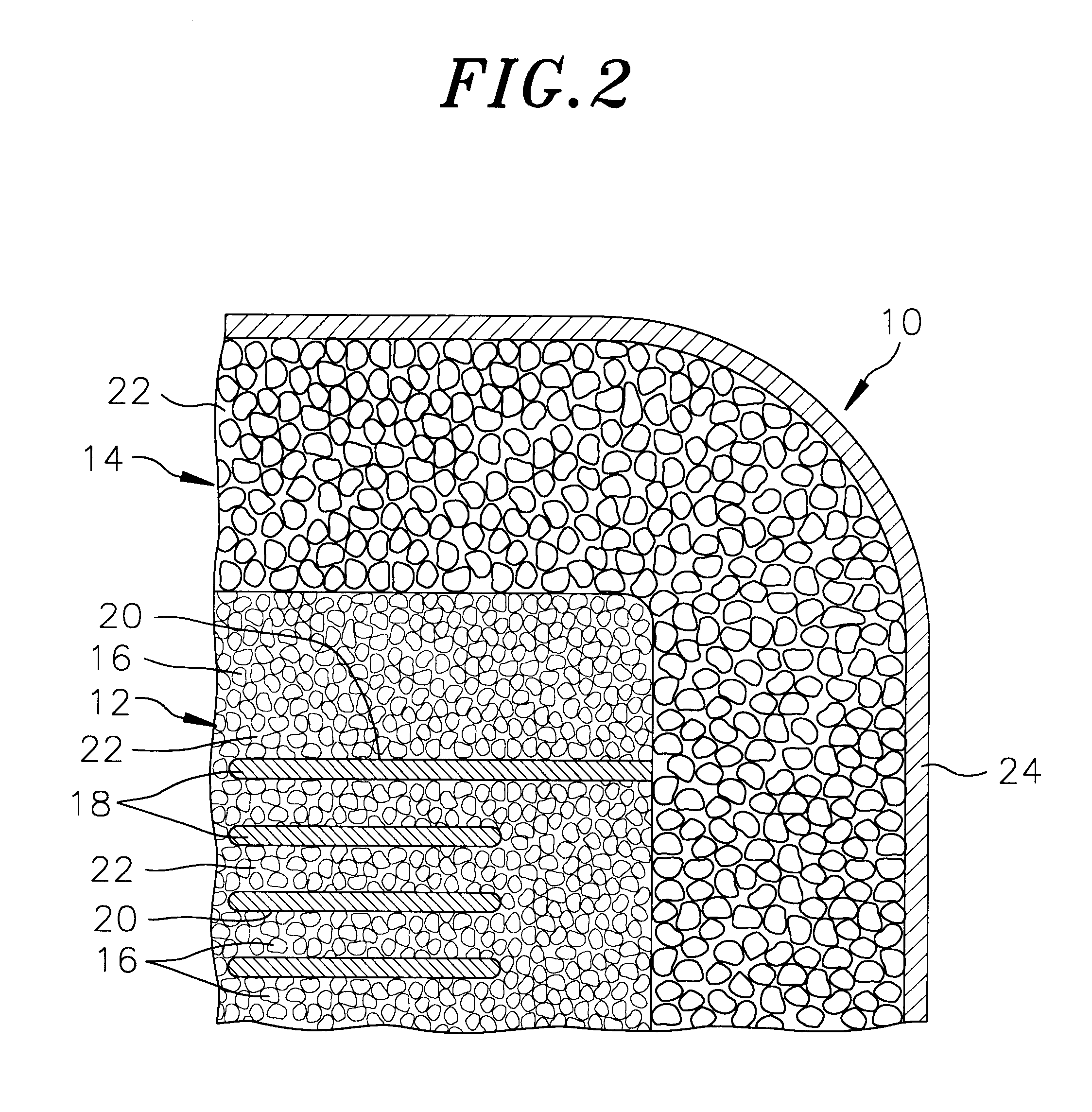
Chip type electronic part and method for the manufacture thereof
a technology of electronic parts and chips, applied in the direction of encapsulation/impregnation, inductance, fixed capacitor details, etc., can solve the problems of internal electrodes vibrating, voids formed between, and chip electric properties degraded
- Summary
- Abstract
- Description
- Claims
- Application Information
AI Technical Summary
Benefits of technology
Problems solved by technology
Method used
Image

Examples
example 2
A main body in Example 2 is formed using the steps described above for Example 1.
Next, silicon resins are impregnated into the magnetic composite material using the steps described hereinbelow: filling a vessel with a silicone resin solution diluted by toluene; immersing a main body in the vessel; putting the vessel in a pressure-control container; lowering the pressure of the container to a pressure of 30 Torr by using a vacuum pump; and maintaining it for 10 minute.
Thereafter, the impregnated main body is removed from the vessel and heat-treated at a temperature of 200.degree. C. for 1 hour so as to harden the impregnated silicone resins impregnated.
Then, the silicone resin adhered to the surface of the main body is removed in a rotating barrel.
Subsequently, a pair of external electrodes is formed on two opposing sides of the main body by coating a conductive paste of a thermosetting epoxy system and hardening it at temperatures of 150.degree. C. for 60 minute and 200.degree. C. f...
PUM
| Property | Measurement | Unit |
|---|---|---|
| pressure | aaaaa | aaaaa |
| temperature | aaaaa | aaaaa |
| thickness | aaaaa | aaaaa |
Abstract
Description
Claims
Application Information