High density programmable read-only memory employing double-wall spacers

a double-wall spacer and read-only memory technology, applied in the field of high-density programmable read-only memory employing double-wall spacers, can solve the problems of large space occupation of eeproms, significant challenge to further increasing the density of arrays, and contact line-to-drain contacts, etc., and achieve the effect of reducing the area

Inactive Publication Date: 2001-07-03
PROMOS TECH INC
View PDF21 Cites 34 Cited by
  • Summary
  • Abstract
  • Description
  • Claims
  • Application Information

AI Technical Summary

Benefits of technology

The present invention provides an EPROM, a flash EPROM, an E.sup.2 PROM and a method for forming the same having increased density. The invention does so by reducing the area after required for formation of a contact. Specifically, a storage cell for electrically programmable read-only memory (EPROM) includes a pair of spaced-apart gate structures, with a double wall spacer structure disposed about each gate structure A dielectric region is disposed atop, and extends coextensive with, each of the pair of spaced apart gate structures. In this manner, a pair of spaced apart insulated gate structures may be formed with an intermetal dielectric layer positioned atop thereof. An aperture is formed in the intermetal dielectric layer so as to be in superimposition with a portion of each of the pair of insulated gate structures and a region of the substrate disposed therebetween. A metallic contact layer, including a plug portion, disposed within the aper

Problems solved by technology

These conventional EEPROM occupy large spaces due to the large capacitive coupling that is required between the floating gate and the control gate.
The metal bit line-to-drain contacts, however, poses a significant challenge to further increasing the density of the array.
This results in increased cell size.
Were the contact mask misaligned, the subsequent e

Method used


Image

  • High density programmable read-only memory employing double-wall spacers
  • High density programmable read-only memory employing double-wall spacers
  • High density programmable read-only memory employing double-wall spacers

Examples


Embodiment Construction

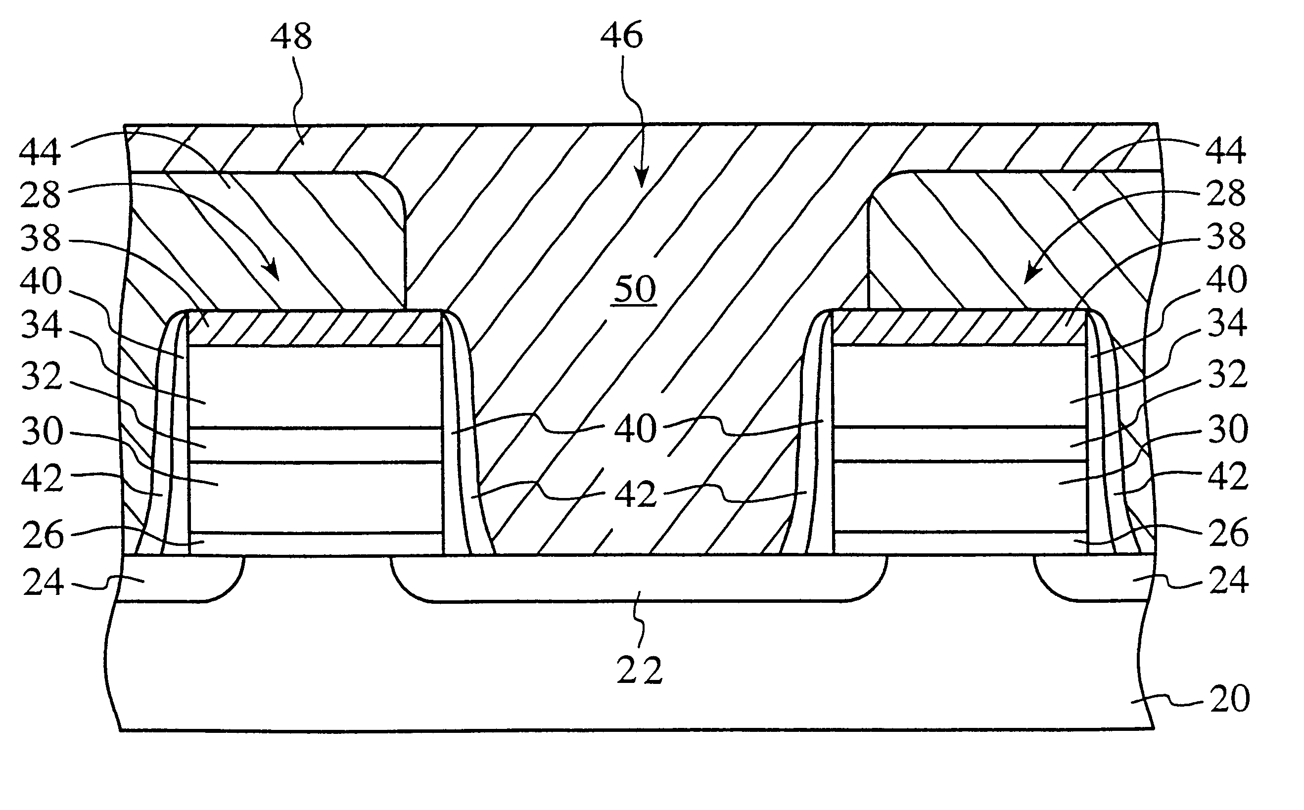
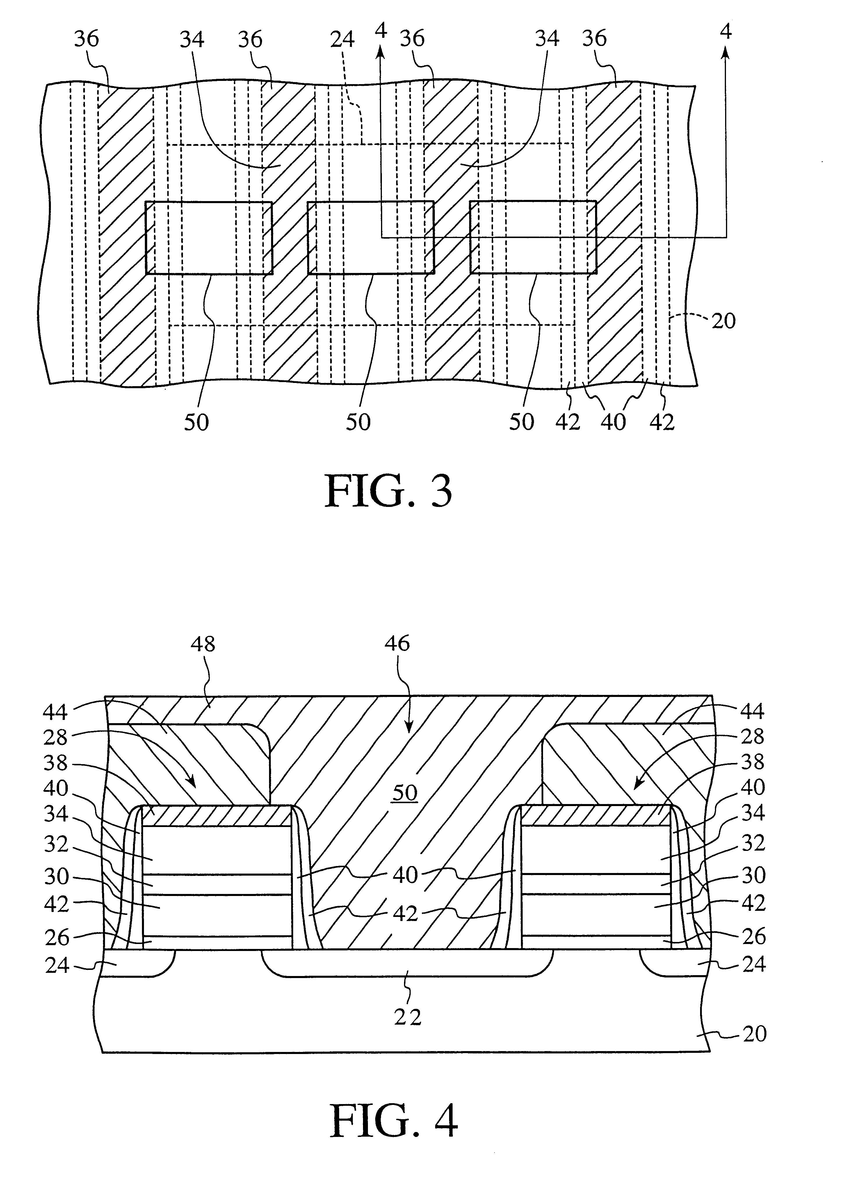
Referring to FIGS. 3 and 4, the EPROM in accord with the present invention may be formed on a silicon substrate 20 that is composed of a P-type doped single crystalline silicon. A relatively thick Field OXide (FOX) 22 is formed on and in portions of the substrate surface surrounding and electrically isolating active devices areas 24. The field oxide 22 may be formed by the LOCal Oxidation of Silicon (LOCOS) method commonly practiced in the semiconductor industry. The LOCOS process includes of depositing, or thermally growing, a thin pad oxide (not shown) composed of silicon oxide on the substrate surface and then depositing a silicon nitride (Si.sub.3 N.sub.4) layer (not shown), usually by chemical vapor deposition (CVD), with the nitride layer serving as a barrier to thermal oxidation. The silicon nitride layer is patterned leaving portions over the silicon substrate where active device regions are required semiconductor devices, such as field effect transistors. The silicon substr...


PUM


Abstract

The present invention provides an EPROM and a method for forming the same having increased density. The invention does so by reducing the area required for formation of a contact. Specifically, a storage cell for an electrically programmable read-only memory having a pair of spaced-apart gate structures, with a double wall spacer structure disposed on opposite sides of each gate structure.

Description

CROSS REFERENCE TO RELATED APPLICATIONSThis application claims priority, pursuant to Title 35, United States Code .sctn.119, from Taiwanese Pat. No. 111452, issued Apr. 10, 1998, and filed on Aug. 6, 1997 as Application No. 86111278 and assigned to Mosel Vitelic, Inc. Taiwanese Pat. No. 111452 is hereby incorporated by reference in its entirety.BACKGROUND OF THE INVENTIONThe present invention relates to the field of semiconductor electronic devices and the method for manufacturing the same. More particularly, the present invention relates to a process suited for manufacturing flash erasable programmable read-only memory cells.Erasable programmable read-only memory (EPROM) technology is well known for use in both memory and programmable logic applications. In particular, EPROMs are implemented using floating gate field effect transistors in which the binary states of the EPROM cell are represented by the presence or absence, on the floating gate, of sufficient charge to prevent condu...

Claims


Application Information

Patent Timeline
IPC IPC(8): H01L27/115H01L21/70H01L21/8247
CPCH01L27/115H01L27/11521H10B69/00H10B41/30
Inventor SUNG, KUO-TUNG
Owner PROMOS TECH INC
Why Eureka
Try Eureka