Wafer level fabrication and assembly of chip scale packages

a technology of chip scale and fabrication, applied in the direction of semiconductor devices, semiconductor/solid-state device details, electrical equipment, etc., can solve the problems of reducing the size of the package, reducing the service life of the package, and increasing the cost of the packag

Inactive Publication Date: 2001-09-04
ROUND ROCK RES LLC
View PDF29 Cites 36 Cited by
  • Summary
  • Abstract
  • Description
  • Claims
  • Application Information

AI Technical Summary

Problems solved by technology

Thus, plastic encapsulated chips may be subject to performance degradation and abbreviated life.
However, the process is more complex and results in an expensive package of increased size.
However, the subsequent etching back of the passivation coating at the bond pads of the semiconductor chip may damage the coating around the bond pads, resulting in a non-hermetic seal and permitting corrosion to deleteriously affect chip reliability and life.
Furthermore, scribing of the wafer prior to metallization of the glass plate is unnecessary.

Method used


Image

  • Wafer level fabrication and assembly of chip scale packages
  • Wafer level fabrication and assembly of chip scale packages
  • Wafer level fabrication and assembly of chip scale packages

Examples


Embodiment Construction

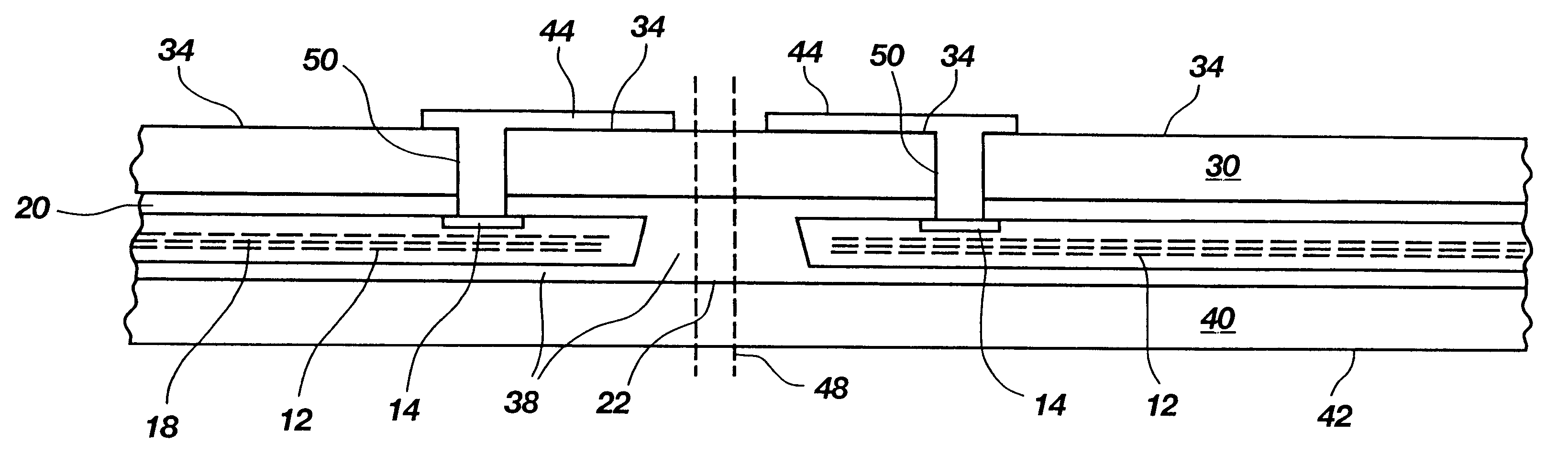
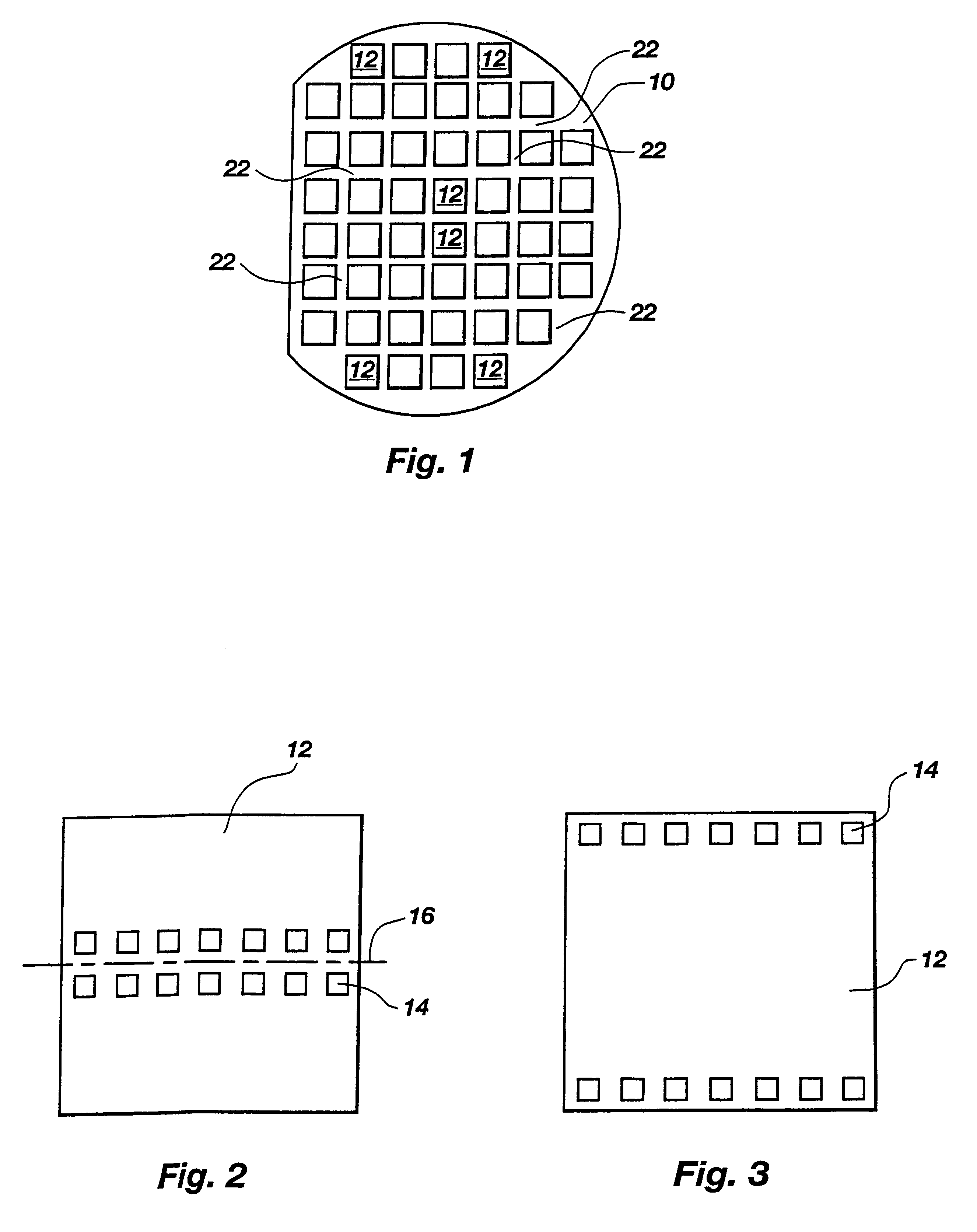
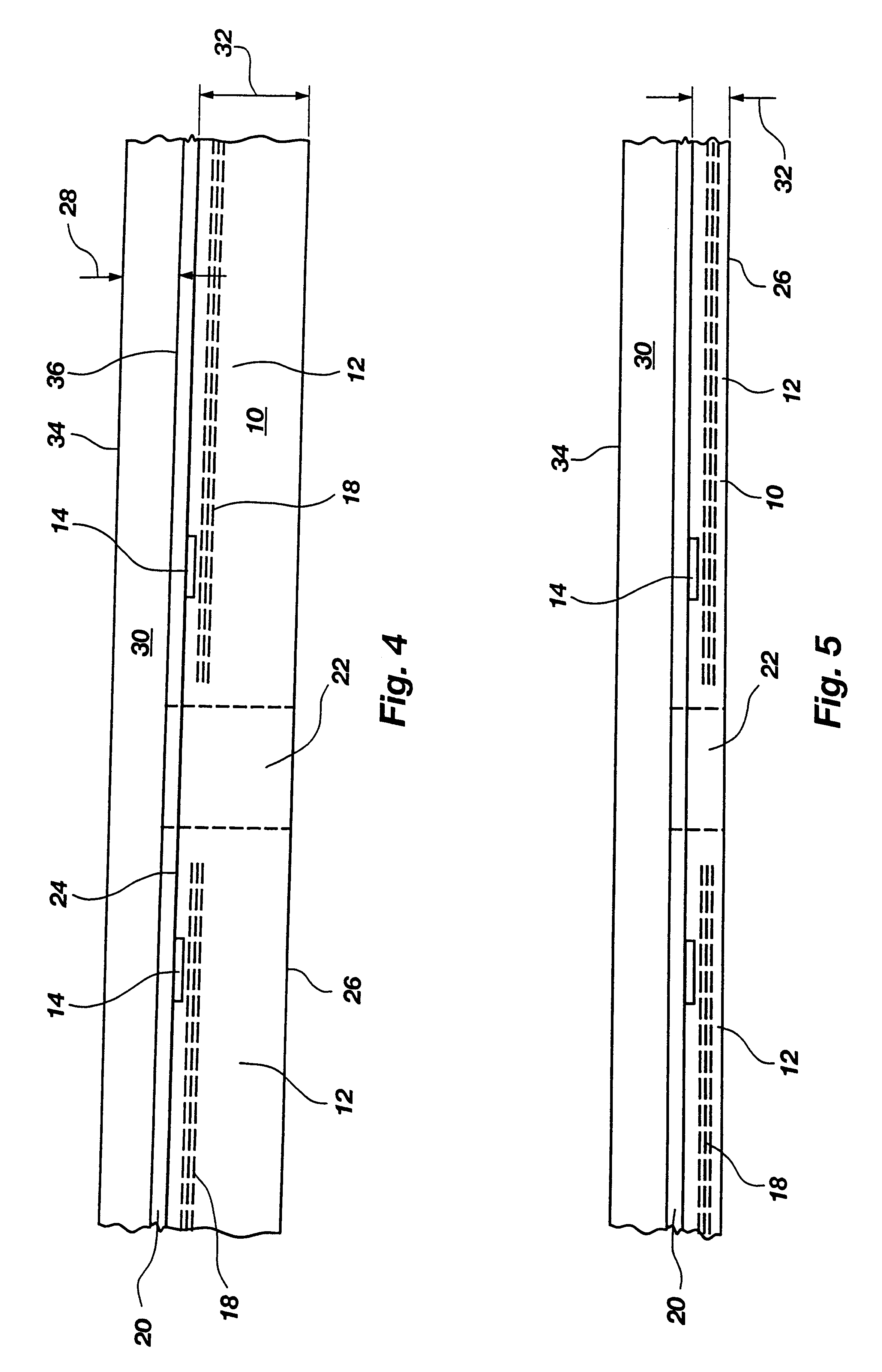
Referring to drawing FIG. 1, a wafer 10 is shown comprising a plurality of semiconductor chips or dice 12 formed thereon. Each semiconductor chip 12 may include a suitable passivation layer or layers (not shown) which is well known in the art for providing a degree of protection for the active circuitry on the chip 12. As shown, the semiconductor chips or dice 12 have not been separated but remain in the form of a wafer 10 for additional wafer processing. While in wafer form, each individual semiconductor chip 12 is distinguished from adjacent chips by generally circuit-free street areas 22 therebetween.

In the following description, the term "silicon" will be used in a generic sense to include other semiconductive materials such as gallium / arsenide or germanium, which are useful for fabricating electronic devices.

As depicted in drawing FIG. 2, a semiconductor chip 12 has a leads-over-chip configuration. Bond pads 14 are connected to circuitry within the chip 12 for access by a host ...


PUM


Abstract

A method for producing integrated circuit devices comprises the steps of forming and packaging such devices at the wafer scale including forming a plurality of chip circuits with bond pads, adhesively fixing a plate of glass to the active surface of the wafer, slicing the wafer, applying a sealant layer to the backside of the wafer, forming contact holes through the upper glass plate, metallizing the glass plate and singulating the individual chips. Use of etchable glass for the package and palladium for metallization provides an advantageous construction method.

Description

1. Field of the InventionThis invention relates to packaged semiconductor devices and methods for manufacture thereof. More particularly, the invention pertains to ultrathin devices having a small footprint and simplified processes for their manufacture including device packaging at the wafer scale.2. Description of the Related ArtSolid state electronic devices, more colloquially known as semiconductor chips or dice, are typically manufactured from a semiconductor material such as silicon, germanium or gallium / arsenide. Circuitry is formed on one surface of the device with input and output (I / O) pads formed around the periphery or centrally positioned to facilitate electrical connection with a host electrical apparatus.A profusion of small electronic consumer products includes pagers, notebook computers, cellular telephones, digital cameras, modems, global position systems and electronic watches, to name a few. The rapidly growing consumer demand for small product size and low profi...

Claims


Application Information

Patent Timeline
Patent Type & Authority Patents(United States)
IPC IPC(8): H01L23/31H01L23/28H01L21/48H01L23/498H01L21/02H01L23/48H01L21/301
CPCH01L21/481H01L23/3107H01L23/49827H01L24/97H01L21/4853H01L2924/01033H01L2224/274H01L2924/01013H01L2924/01029H01L2924/0103H01L2924/01032H01L2924/01039H01L2924/01046H01L2924/01074H01L2924/01075H01L2924/01078H01L2924/01082H01L2924/14H01L2924/01005H01L2924/01006H01L2924/01023H01L24/19H01L2224/04105H01L2224/32225H01L2224/92144
Inventor FARNWORTH, WARREN M.
Owner ROUND ROCK RES LLC
Why Eureka
Try Eureka