Method for making cards with multiple contact tips for testing semiconductor chips

a technology of semiconductor chips and contact tips, which is applied in the direction of cable/conductor manufacturing, decorative arts, ion implantation coating, etc., can solve the problems of limited placement of tips on these known cards, and no longer in keeping with the constant progress

Inactive Publication Date: 2001-09-18
MESATRONIC
View PDF15 Cites 54 Cited by
  • Summary
  • Abstract
  • Description
  • Claims
  • Application Information

AI Technical Summary

Problems solved by technology

Placing of the tips on these known cards is nevertheless limited to a given number of tips, which is no longer in keeping with the constant progress as far as integration of semiconductor chips is concerned.

Method used


Image

  • Method for making cards with multiple contact tips for testing semiconductor chips
  • Method for making cards with multiple contact tips for testing semiconductor chips
  • Method for making cards with multiple contact tips for testing semiconductor chips

Examples


Embodiment Construction

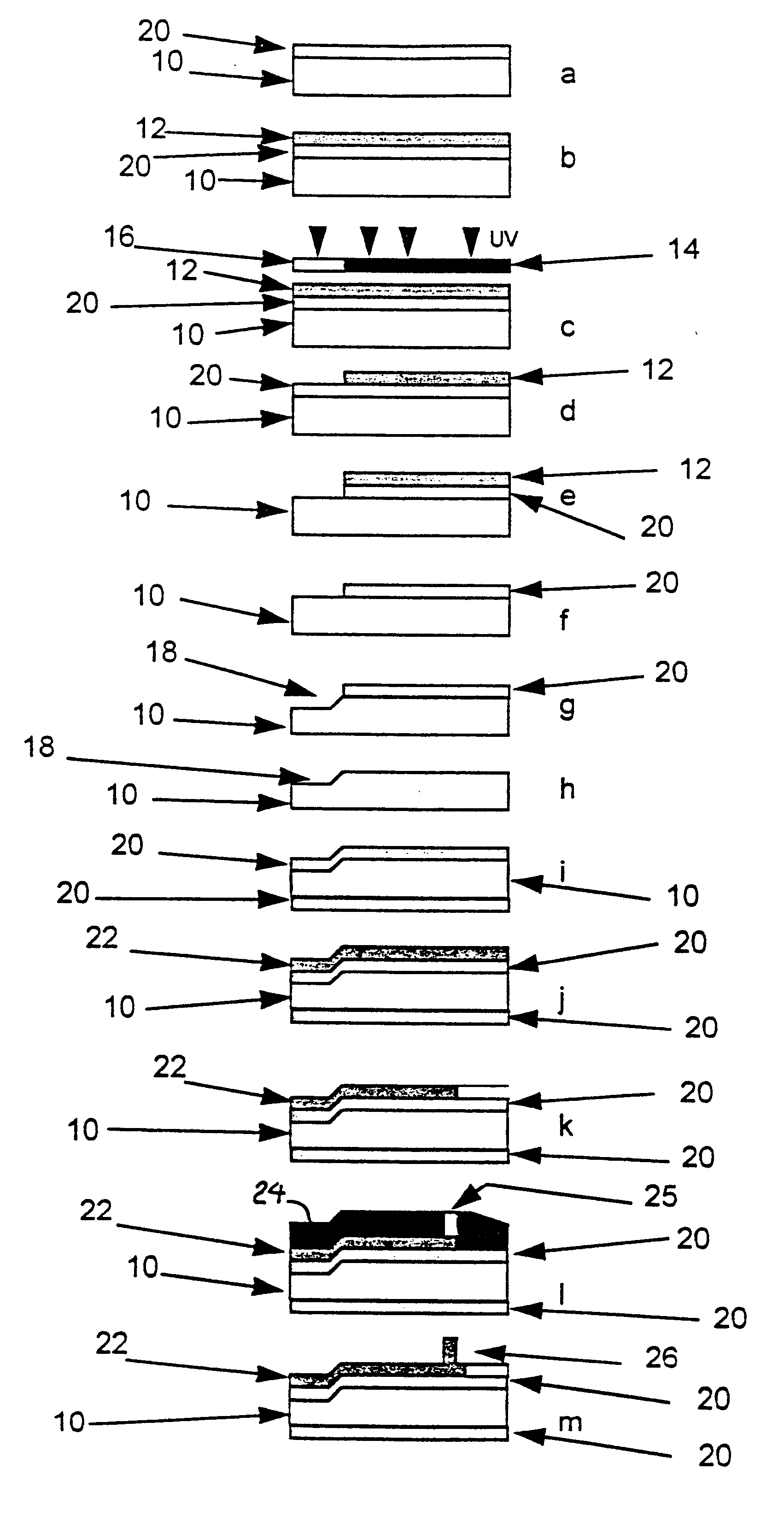
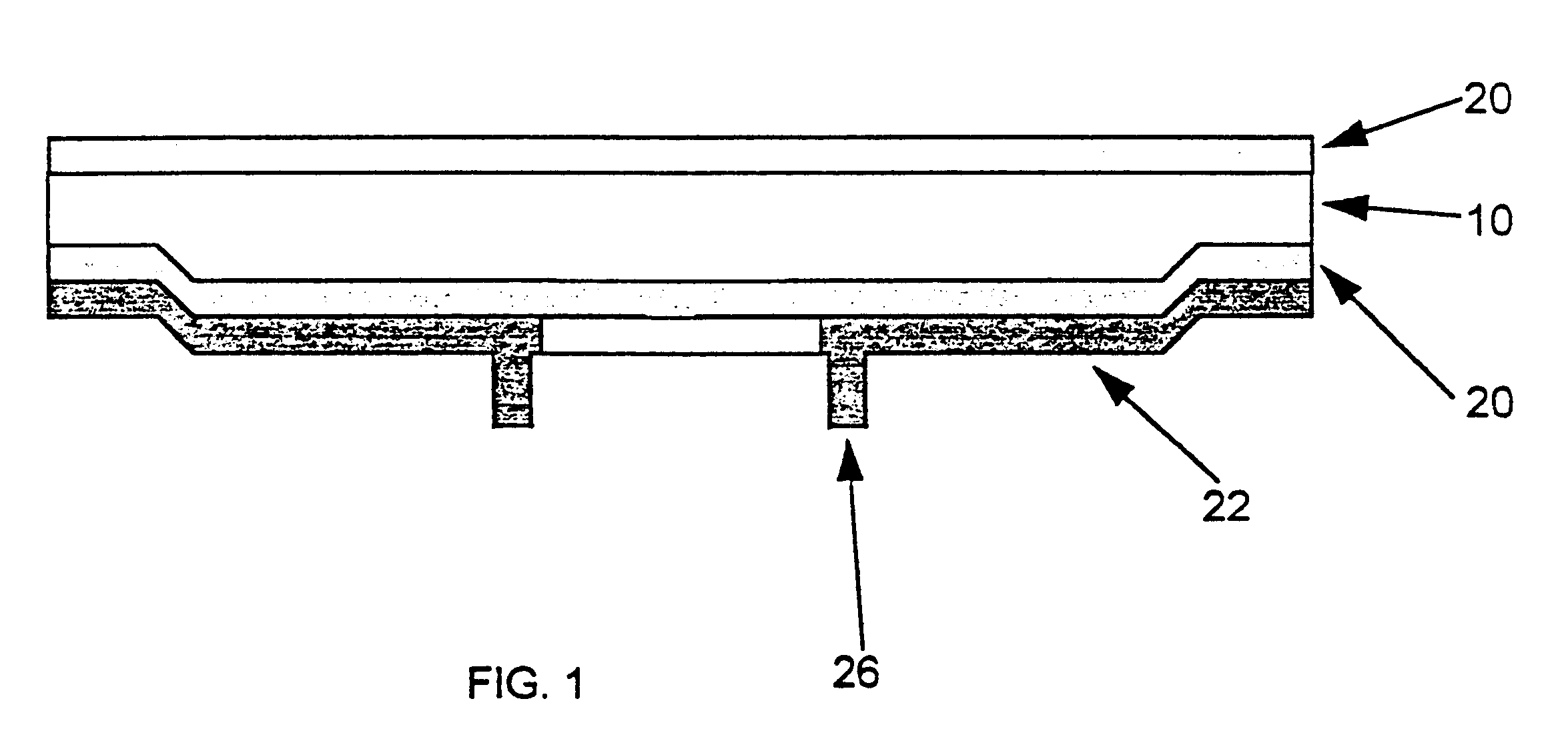
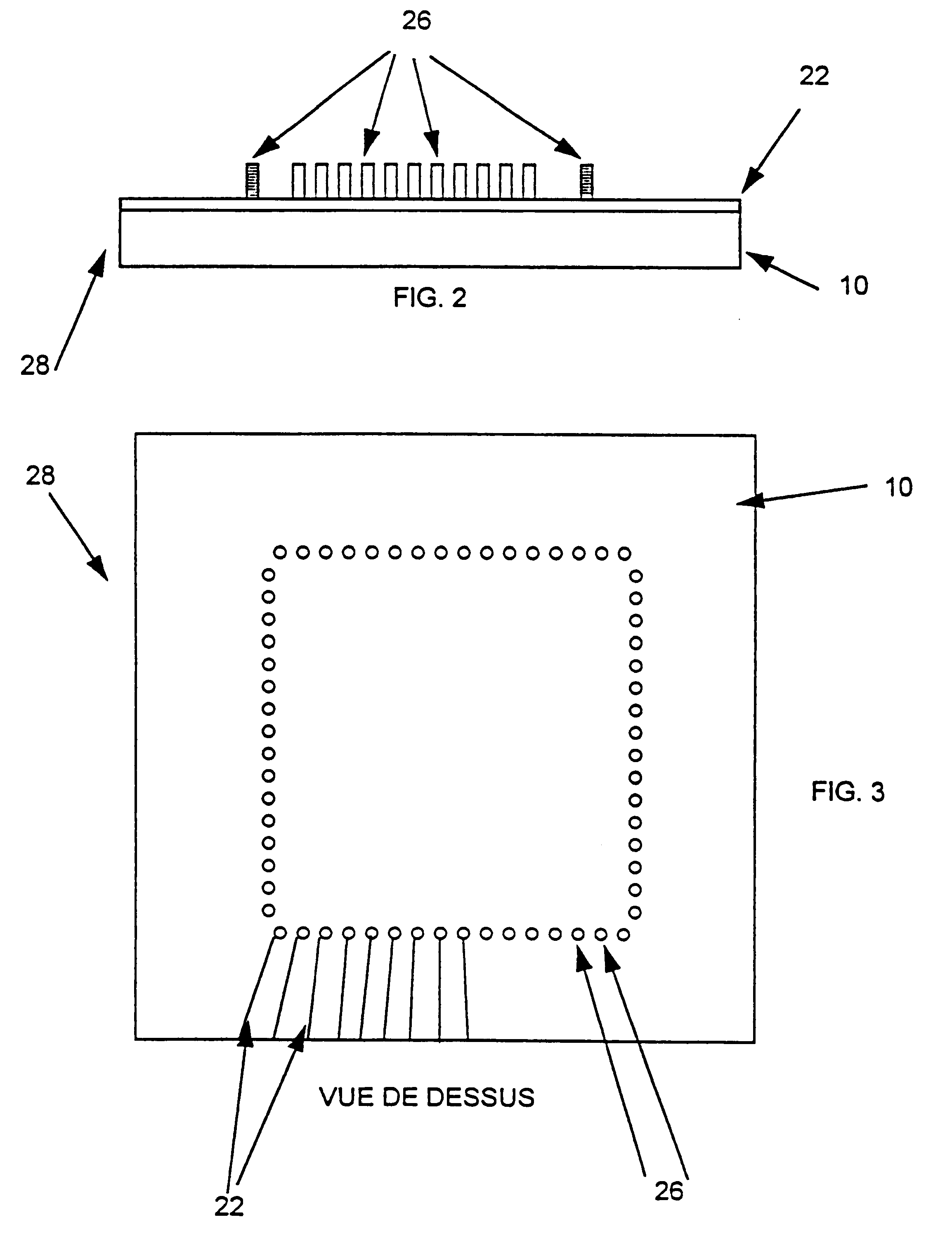
The different stages of the example of the process for implementation of the multiple tip card for checking chips after manufacturing are illustrated in the drawing of FIG. 12 for indicative purposes.

Stage a:

Starting from a monolithic substrate 10 made of oxidised silicon an insulating layer 20 is formed. The substrate is compatible with the UV photolithography technique enabling required precisions to be obtained, in particular under a micron. Other materials can naturally be used to form the substrate 10, in particular Gallium Arsenide As Ga, quartz, or glass.

Stage b:

The substrate 10 is coated with a photosensitive resin 12 so as to obtain a uniform layer.

Stage c:

A first UV photolithography operation is then performed consisting in producing a local insulation of the resin 12 of the upper layer through a mask 14 having a hole 16 of predetermined shape. The UV radiation is generated by means of an ultraviolet lamp placed above the mask 14.

Stage d:

The insulated resin 12 is dissolved...


PUM

PropertyMeasurementUnit
current densityaaaaaaaaaa
diameteraaaaaaaaaa
depthaaaaaaaaaa

Abstract

The invention relates to a process for manufacturing a card with multiple tips, designed in particular for testing semiconductor chips or integrated circuits before encapsulation thereof and comprising an oxidised silicon substrate 10 on the two opposite surfaces, one of the surfaces being provided with conducting strips connected to contacts in the form of tips 26. A thin metal layer 22 is deposited by vapour deposition in a vacuum or by cathode sputtering on one of the insulated surfaces of the monolithic substrate 10, and the conducting strips are obtained by means of a UV photolithography operation making use of a photosensitive resin, followed by etching of the thin metal layer 22 according to the location and shape of the tips 26. Another UV photolithography operation is then performed consisting in depositing a thick layer 24 of photosensitive resin on the thin etched layer, the resin then being revealed with the drawing 25 of the tips. The tips 26 are finally obtained by electroforming by means of a bath containing metal ions enabling electroformed pads corresponding to the shape of the drawings 25 to be achieved.

Description

1. Field of the InventionThe invention relates to a process for manufacturing a card with multiple tips, designed in particular for testing semiconductor chips or integrated circuits before encapsulation thereof and comprising a substrate one of the surfaces of which is provided with conducting strips connected to contacts in the form of tips.2. Description of Related ArtCards with tips are used for checking chips or integrated circuits after manufacturing and prior to encapsulation. Cards known up to now generally use different types of technologies, i.e. soldered blade tip cards, epoxy ring cards, and membrane cards, as described in the documents EP-A-0475050, WO 9409374 and EP-0646800. Placing of the tips on these known cards is nevertheless limited to a given number of tips, which is no longer in keeping with the constant progress as far as integration of semiconductor chips is concerned.The document WO 96 / 36884 describes a manufacturing process of a card subjected to prior cutt...

Claims


Application Information

Patent Timeline
Patent Type & Authority Patents(United States)
IPC IPC(8): G01R1/067G01R1/073G01R3/00H01L21/66H05K3/00
CPCG01R3/00G01R1/07342G01R1/06733Y10T29/49117
Inventor BELMONT, ANDREREYNAUD, VINCENTDANIAU, WILLIAM
Owner MESATRONIC
Why Eureka
Try Eureka