Content addressable memory system with cascaded memories and self timed signals

a memory system and cascade technology, applied in memory adressing/allocation/relocation, digital storage, instruments, etc., can solve the problems of system storage requirements exceeding the number of entries stored, less robust design, and difficult to prevent bus contention

Inactive Publication Date: 2001-10-09
FOOTHILLS IP LLC +1
View PDF11 Cites 79 Cited by
  • Summary
  • Abstract
  • Description
  • Claims
  • Application Information

AI Technical Summary

Problems solved by technology

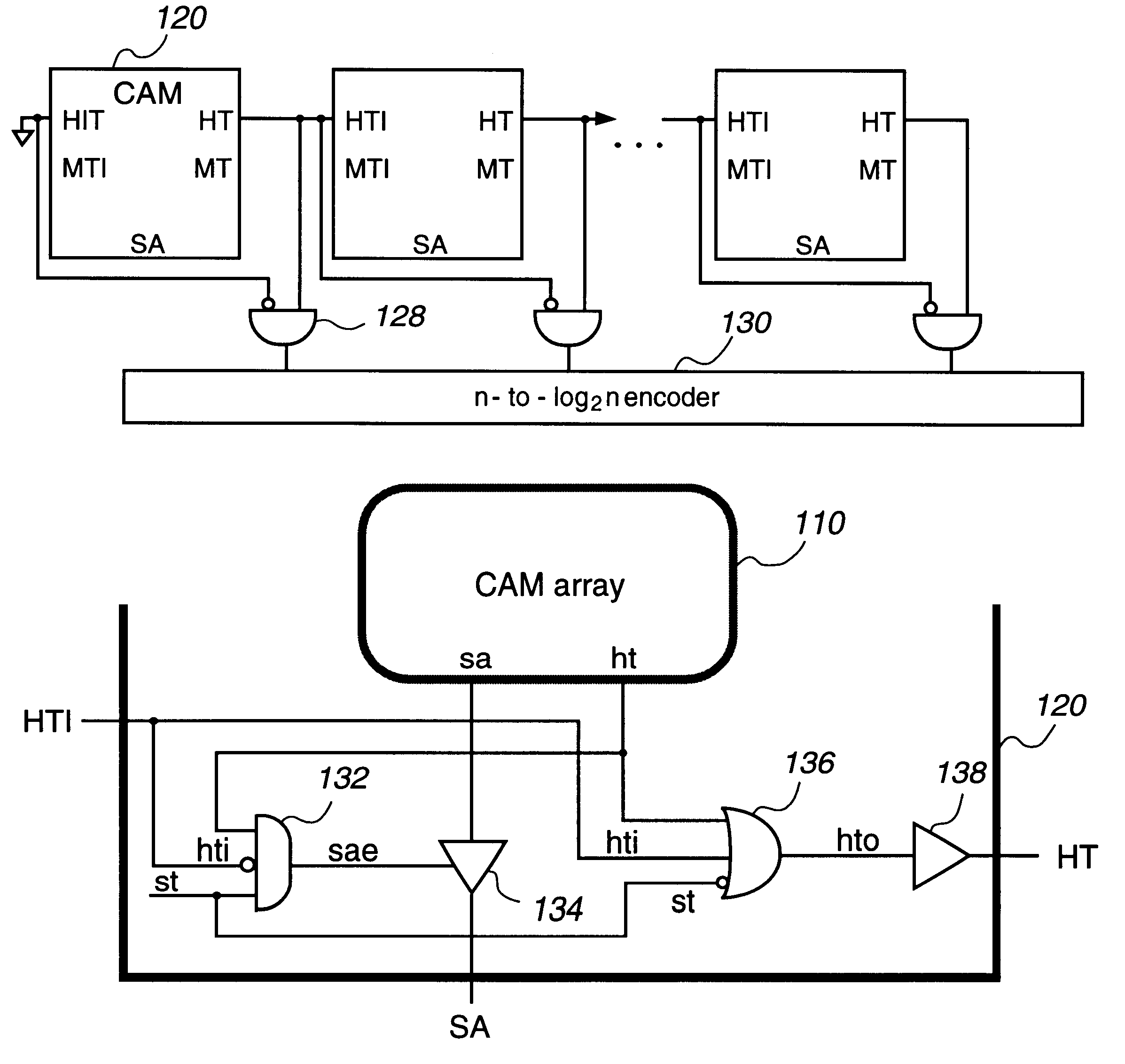
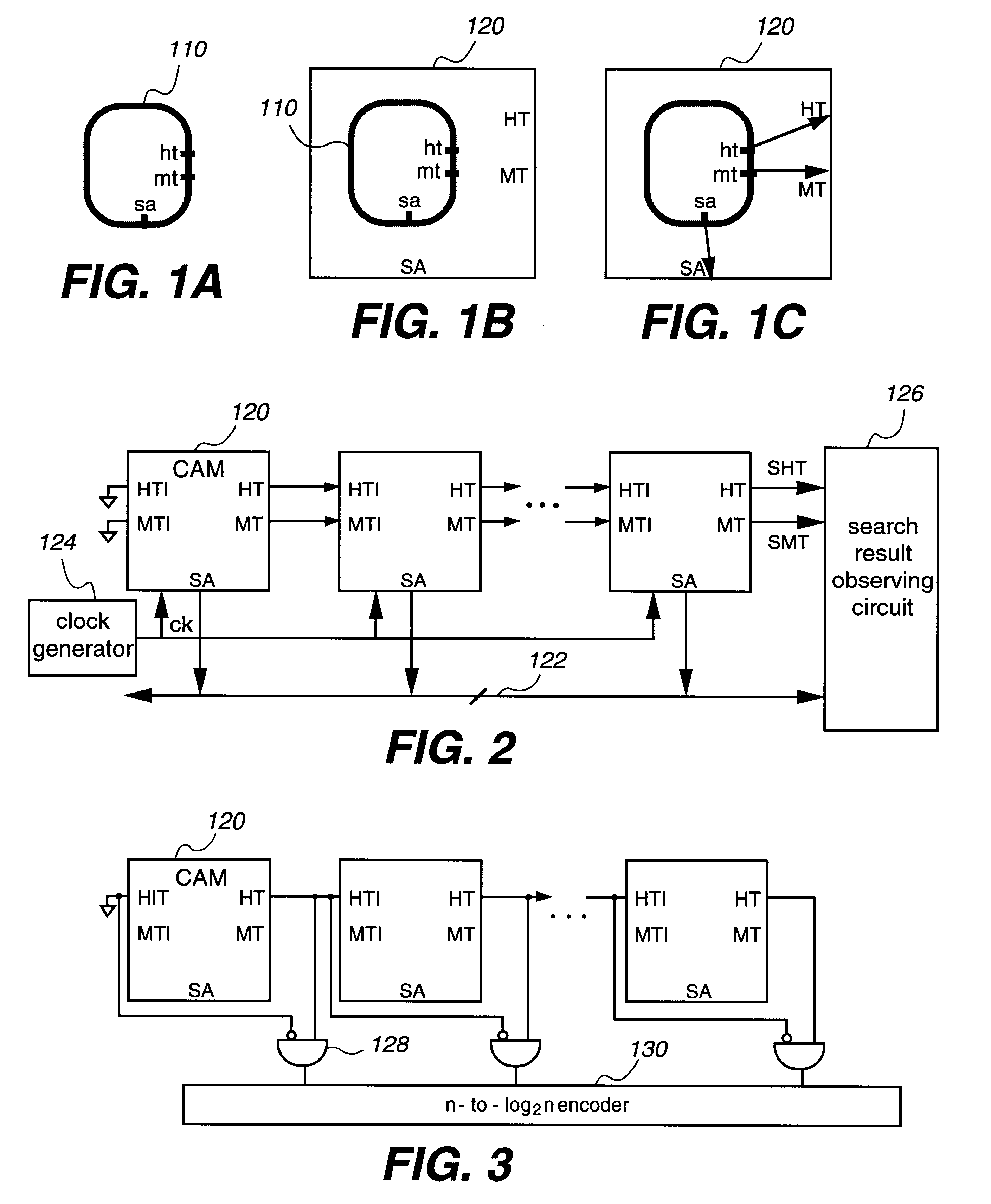
Often, system storage requirements exceed the number of entries stored on a single CAM chip.
Note that such an approach would lead to a less robust design.
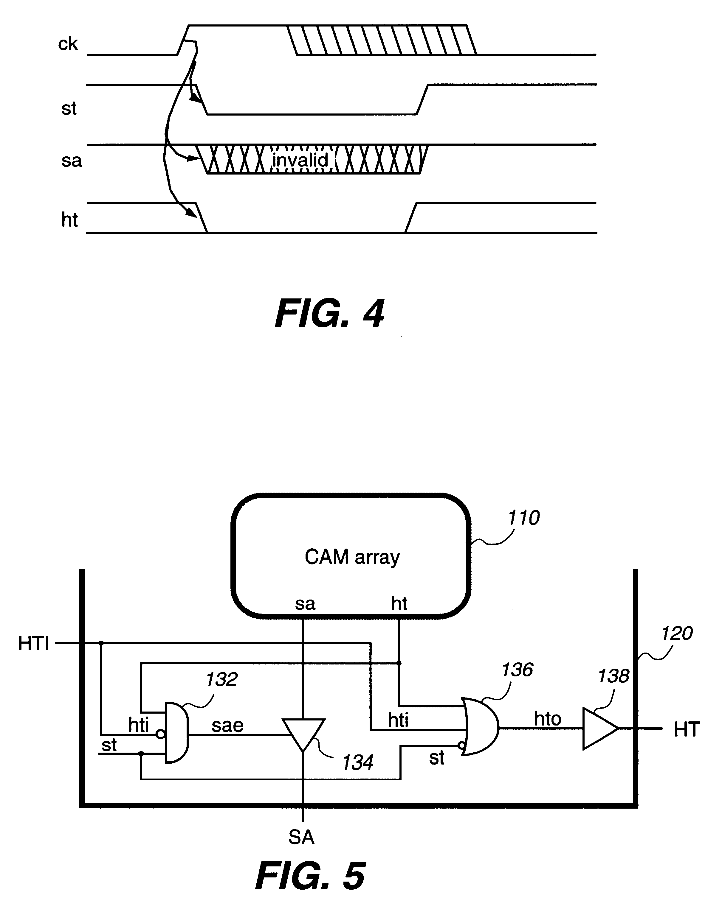
Bus contention would be difficult to prevent, and disable timing would depend on a chip's position in the cascade.

Method used


Image

  • Content addressable memory system with cascaded memories and self timed signals
  • Content addressable memory system with cascaded memories and self timed signals
  • Content addressable memory system with cascaded memories and self timed signals

Examples


fifth example

VII-5. Fifth Example

FIG. 15 is a block diagram of a circuit using a plurality of word slices using the same match logic as the second CAM array where a self-timed signal generation in this arrangement employs a model global data line.

A fifth example of the self-timed signal generator can be used to track hit delay in a CAM array with a plurality of the vertical word slices employed in the second CAM array, as shown in FIG. 15. The plurality of word slices allows the realization of larger capacities. Because all bits of the comparand D must be bused to all word slices, a global data bus 622 is employed. Timing information may be embedded in a global data bus 622, in the form of a model global data line 624. The model global data line 624 is driven such that its first transition approximately coincides with the downward transition of the hit signal ht. The model global data line 624 is also used to provide timing information to the CAM array, guaranteeing this coincidence. The falling...


PUM


Abstract

A system includes cascaded content addressable memory (CAM) chips connected to a common bus. Each CAM chip includes a CAM array, a self-timed signal generator and hit propagation and match address transfer circuits. Each CAM array including an array of core cells provides, through its encoder, hit and match address signals resulting from a search operation in response to a clock signal. Each match address transfer circuit transfers the match address signal to the common bus, in response to a self-timed signal, the hit signal and a propagation-in hit signal provided from an upstream CAM chip, so that more than one CAM chip is prevented from providing the match address signal to the common bus simultaneously. Each hit propagation circuit provides a propagation-out hit signal to a downstream CAM chip, in response to the self-timed signal, the hit signal and the propagation-in hit signal from the upstream CAM chip, so that a hit signal is propagated from an upstream CAM chip to a downstream CAM chip. Each CAM chip may include an extra row for providing a modelmiss signal or a modelhit signal which is used for a generating self-timed signal. Each word may be divided into two halves and two match lines of the two halves are coupled by a logic circuit. The system may also observe a multiple match status and the highest priority chip indicating a match.

Description

The present invention relates to a content addressable memory (CAM) system in which a plurality of CAM chips are cascade-connected.BACKGROUND INFORMATIONIn known CAMs, data is selected based on contents, rather than physical location. This function is useful for many applications, especially when performing a look-up for the purposes of mapping a long identification word data to a shorter word data. This operation is required in many telecommunications (telecom) functions, including Asynchronous Transfer Mode (ATM) address translation.Often, system storage requirements exceed the number of entries stored on a single CAM chip. Multiple chips are then required, and it is necessary that a means be developed to cascade these multiple chips such that they may be searched as a single entity. An appropriate "user-friendly" cascading capability enables the same chip to be used in a range of systems with different capacity requirements, and allows for easy expandability and scalability, as w...

Claims


Application Information

Patent Timeline
Patent Type & Authority Patents(United States)
IPC IPC(8): G11C15/00G11C15/04
CPCG11C15/04G11C11/34
Inventor SCHULTZ, KENNETH JAMESSHAFAI, FARHADGIBSON, GARNET FREDERICK RANDALL
Owner FOOTHILLS IP LLC
Why Eureka
Try Eureka