Semiconductor device and a method of manufacturing the same

a semiconductor and film-forming technology, applied in semiconductor devices, instruments, optics, etc., can solve the problems of poor interlayer coverage, inconvenient thickening of the film, and insufficient capacitance of those alon

Inactive Publication Date: 2001-11-06
SEMICON ENERGY LAB CO LTD +1
View PDF32 Cites 136 Cited by
  • Summary
  • Abstract
  • Description
  • Claims
  • Application Information

AI Technical Summary

Problems solved by technology

However, the capacitance having those alone is not large enough and hence is ordinarily supplemented with a storage capacitance (also called as Cs) formed separately from the former.
However, such a structure may have a problem of poor coverage of the interlayer insulating film 202 at an end por

Method used


Image

  • Semiconductor device and a method of manufacturing the same
  • Semiconductor device and a method of manufacturing the same
  • Semiconductor device and a method of manufacturing the same

Examples


embodiment 1

[Embodiment 1]

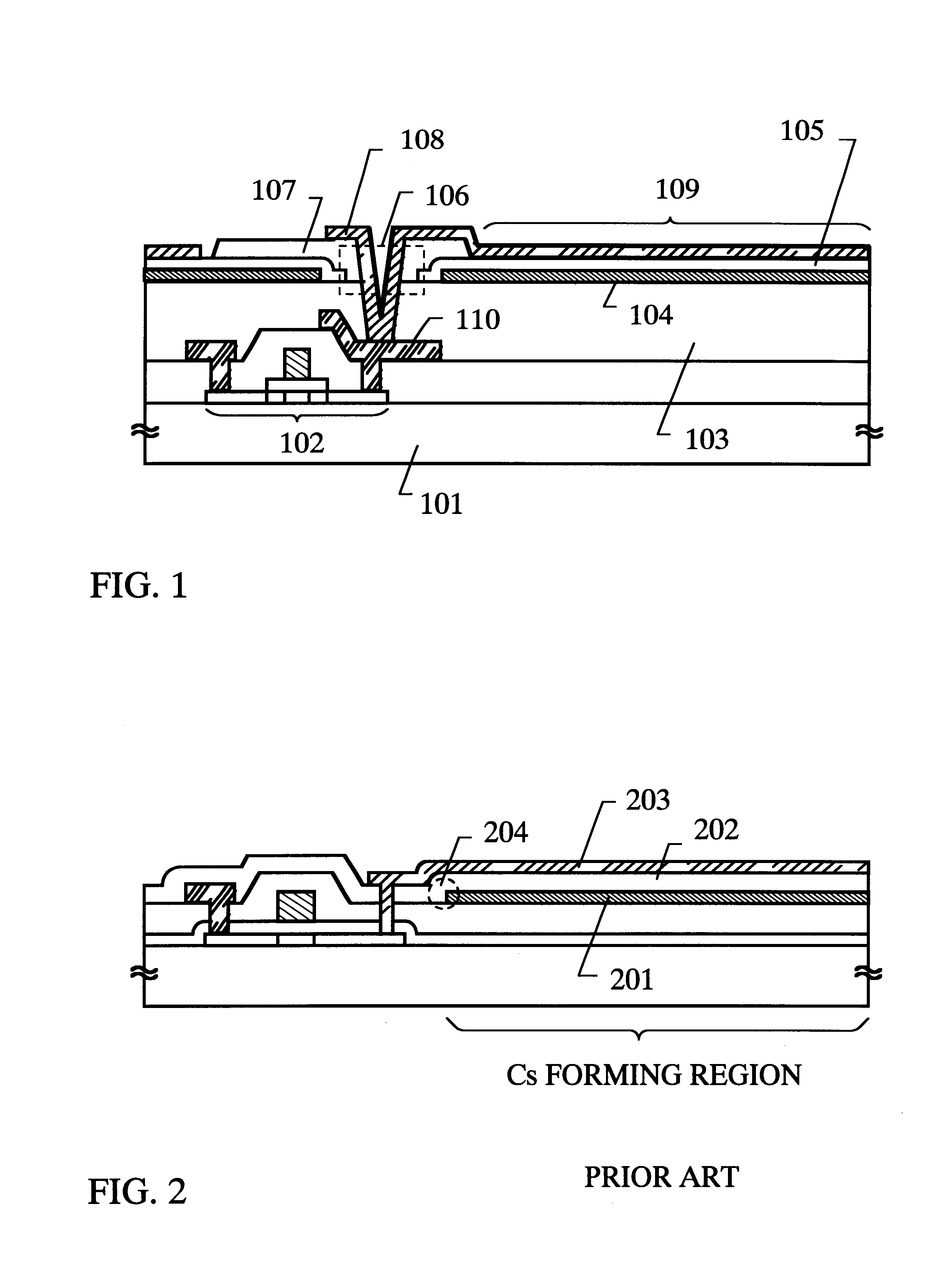
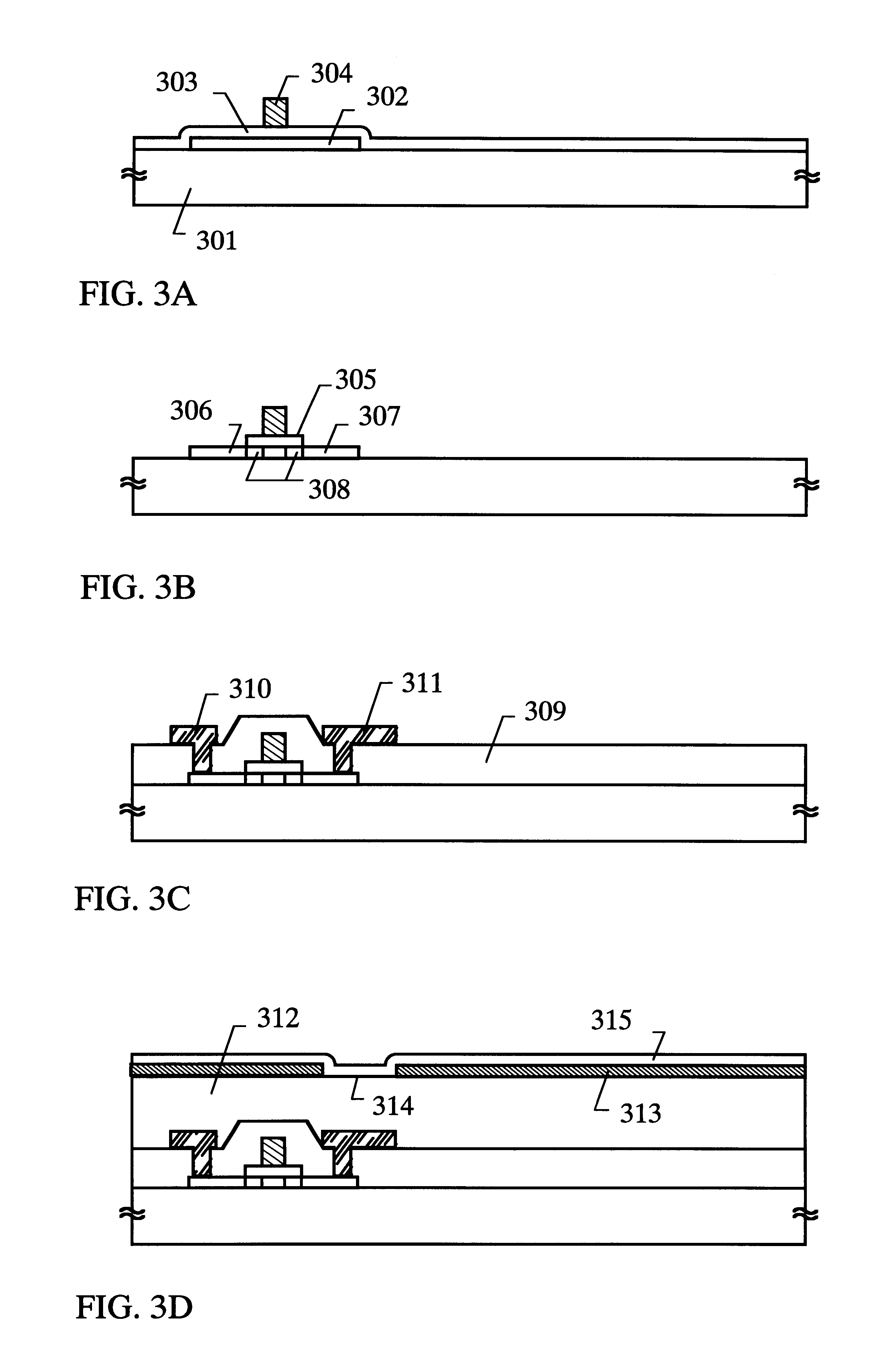
In this embodiment, a process example of manufacturing an active matrix type liquid crystal display device is described with reference to FIGS. 3A to 3D, 4A to 4D, 6, 15A to 15C and 16. It is needless to say that though the description in this embodiment is made focusing on one pixel in a pixel matrix circuit, a driver circuit and a signal processing circuit can also integrally formed on the same substrate.

Firstly, a glass substrate provided with on its surface a base film made of silicon oxide is prepared as a substrate 301 having an insulating surface. Other than a glass substrate, may of course be used a quartz substrate (not necessarily provided with a base film), a ceramic glass substrate or a silicon wafer on which a thermal oxide film is formed. If the heat resistance and the process temperature are balanced, a plastic substrate may also be used.

The structure also effective is such that a heat radiating layer such as a metal film or aluminum nitride film is prov...

embodiment 2

[Embodiment 2]

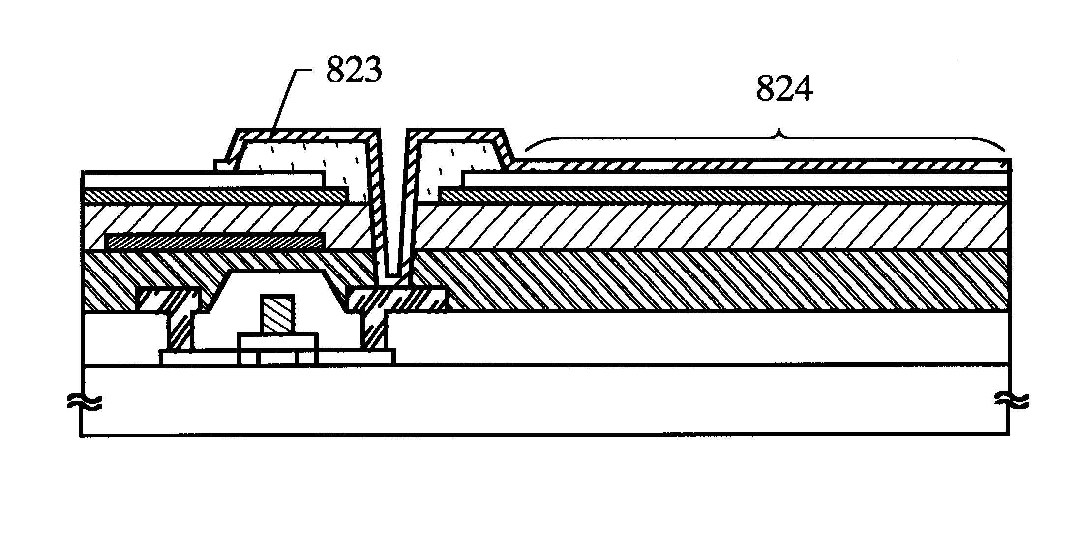
In this embodiment, in the structure shown in FIG. 1, a resin material having light shielding property (representatively a black resin material) is used as the insulating film 107, which is utilized as a black mask. The structure of this embodiment is a modified one of FIG. 1, in which merely a raw material for the insulating film 107 shown in FIG. 1 is changed, and the structure shown in this embodiment is readily realized by following the manufacturing process shown in Embodiment 1.

In this embodiment, a resin material in which black pigment, a metal material (titanium, chromium or the like) or a carbon-based material (such as graphite) is dispersed may be used as a black resin material. However, to utilize it as a black mask, the material desirably has an OD value of 3 or more. This embodiment employs a resin material (with OD value of 3) in which graphite is dispersed.

The OD value is the index representing light shielding property of a thin film, and is expressed wi...

embodiment 3

[Embodiment 3]

In this embodiment, the structure in which a transparent resin material such as acryl or polyimide, and a black resin material, described in Embodiment 2, are laminated is employed instead of the interlayer insulating film 107 of FIG. 1. Incidentally, the structure of this embodiment also, as in Embodiment 2, may be readily realized by following the manufacturing process of Embodiment 1.


PUM


Abstract

In a liquid crystal display device, an improved storage capacitance that uses a pair of transparent conductive films for electrodes is provided. On a flattening film made of a resin, a first transparent conductive film and an insulating film for capacitance are formed into a lamination to form in this laminated film an opening portion. An insulating film covering near the opening portion is formed. A transparent conductive film is formed and patterned to form a pixel electrode. Thus is formed a storage capacitance having the structure where the insulating film for capacitance is sandwiched between the first transparent conductive film and the pixel electrode.

Description

1. Field of the InventionThe present invention relates to an electro-optical device represented by a liquid crystal display device, and to the structure of an electronic apparatus provided with as a part such an electro-optical device. Incidentally, the term "semiconductor device" in this specification designates devices in general which can function with the use of characteristics of semiconductor, and therefore the above-described electro-optical device and electronic apparatus fall into the semiconductor devices.2. Description of the Related ArtIn recent years, what has received attention is an active matrix type liquid crystal display device in which a circuit is consisted of a thin film transistor (hereinafter, referred to as TFT) utilizing a polysilicon film. This is a device intended for realization of image display with high definition by, using a plurality of pixel TFTs that are arranged in matrix, controlling on matrix basis the electric field that applies on the liquid cr...

Claims


Application Information

Patent Timeline
IPC IPC(8): G02F1/13G02F1/1362H01L27/10
CPCG02F1/136213G02F1/136227H01L27/10
Inventor OHTANI, HISASHINAKAZAWA, MISAKO
Owner SEMICON ENERGY LAB CO LTD
Why Eureka
Try Eureka