Semiconductor device and method for producing the same

a technology of thin film transistor and semiconductor device, which is applied in the direction of semiconductor device, electrical apparatus, transistor, etc., can solve the problems of inferior tft based on amorphous silicon film, inability to manufacture cmos circuits, and limited substrate type of materials

Inactive Publication Date: 2001-11-13
SEMICON ENERGY LAB CO LTD
View PDF77 Cites 37 Cited by
  • Summary
  • Abstract
  • Description
  • Claims
  • Application Information

AI Technical Summary

Problems solved by technology

In addition, although the peripheral driver circuit is generally constructed by a CMOS circuit, there is a problem that a CMOS circuit cannot be fabricated, because the properties of a P-channel TFT based on an amorphous silicon film are too inferior as compared with those of an N-channel TFT.
Thus, a type of material of the substrate is limited.
However, since distinct shrinking and warping appear on a glass substrate when it is heated at 600.degree. C. or higher, a glass substrate can not be used practically in a process having heating treatment at 600.degree. C. or higher.
Thus, if heating treatment at a temperature higher than the deformation temperature is performed for the Corning 7059 glass substrate, a large warping or shrinking occurs on the substrate to make it practically unapplicable.
However, a quartz substrate is very expensive, and it costs 10 times as high as the price of a glass substrate.
Thus, a quartz substrate is economically unfeasible.
In the physical method, it is difficult to uniformly form an extremely thinner film on the amorphous silicon film.
Thus, since the metal element can not be brought in uniform contact with the amorphous silicon film, its distribution becomes unbalanced easily during the crystal growth.

Method used


Image

  • Semiconductor device and method for producing the same
  • Semiconductor device and method for producing the same
  • Semiconductor device and method for producing the same

Examples


example 2

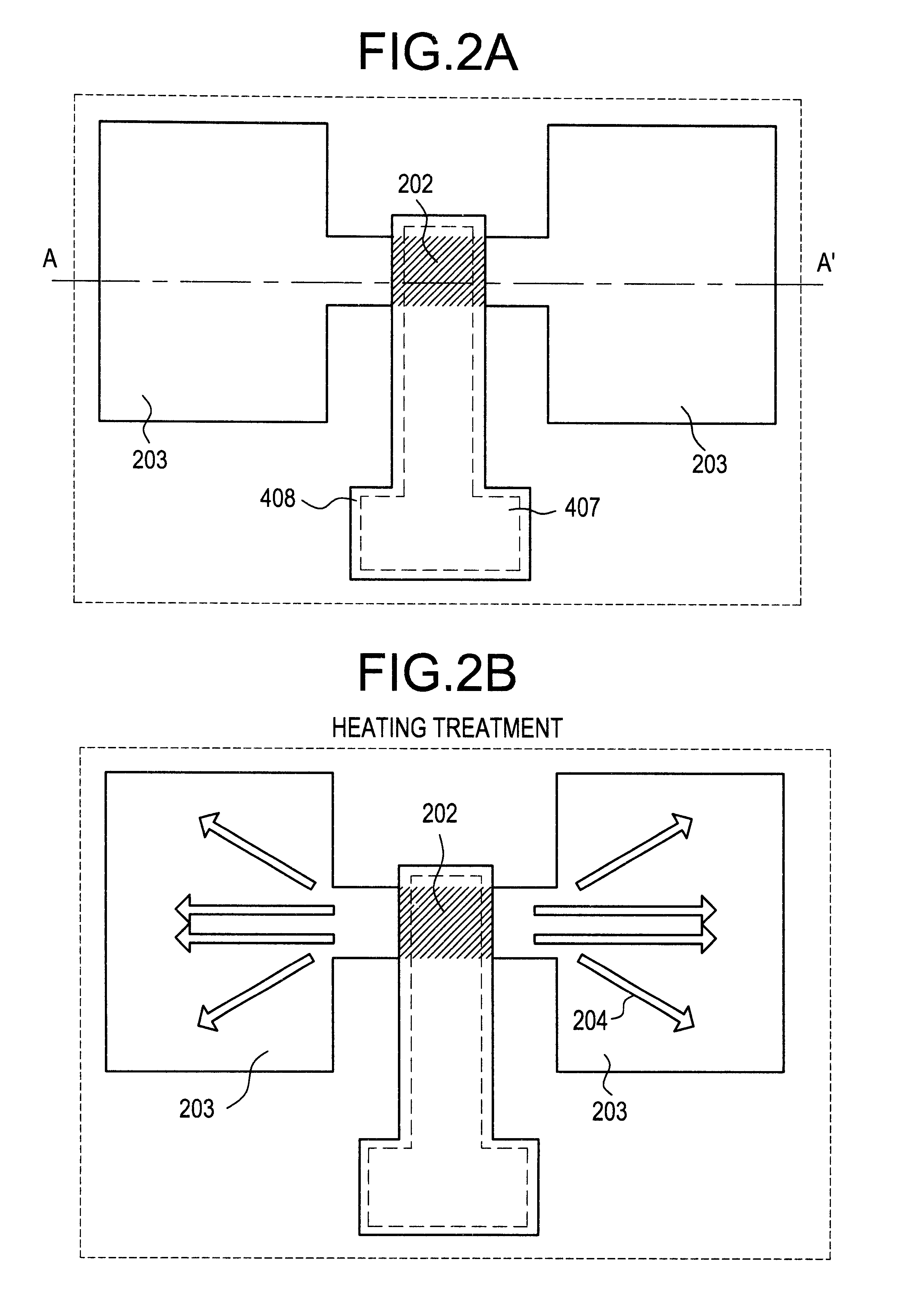
The present example is similar to Example 1, except for forming the gate electrode 407 with silicon or a silicide (a compound of a metal with silicon). In FIG. 5A, the heating treatment can be performed at the crystallization temperature of amorphous silicon or higher, i.e., 450.degree. C. or higher. However, the heating treatment must be effected at a temperature not higher than the deformation temperature of the glass substrate, for instance, at 550.degree. C. By the heating treatment, as shown in FIG. 2B, the region 203 once rendered amorphous is crystallized, and nickel element diffuses out from the crystalline region 202 along the progressive direction of crystal growth. Finally, nickel element is found to concentrate in the end portion of the region 203.

The later steps can be effected in a similar manner as those described in Example 1, to complete a TFT.

example 3

The present example is an example of a method for performing heating treatment to allow the crystals grow from the region into which the metal element for accelerating the crystallization of silicon is introduced, and then producing a TFT using the obtained region. The producing method of the example differs from that described in Example 1 in two aspects; one is concerned with the relation between the region into which the metal element is introduced and the region to be crystallized, and the other is concerned with the morphology of the crystallized portion.

In the example, the region into which the metal element is introduced is crystallized, and then the active layer (channel forming region) of the TFT is produced by using the crystallized region.

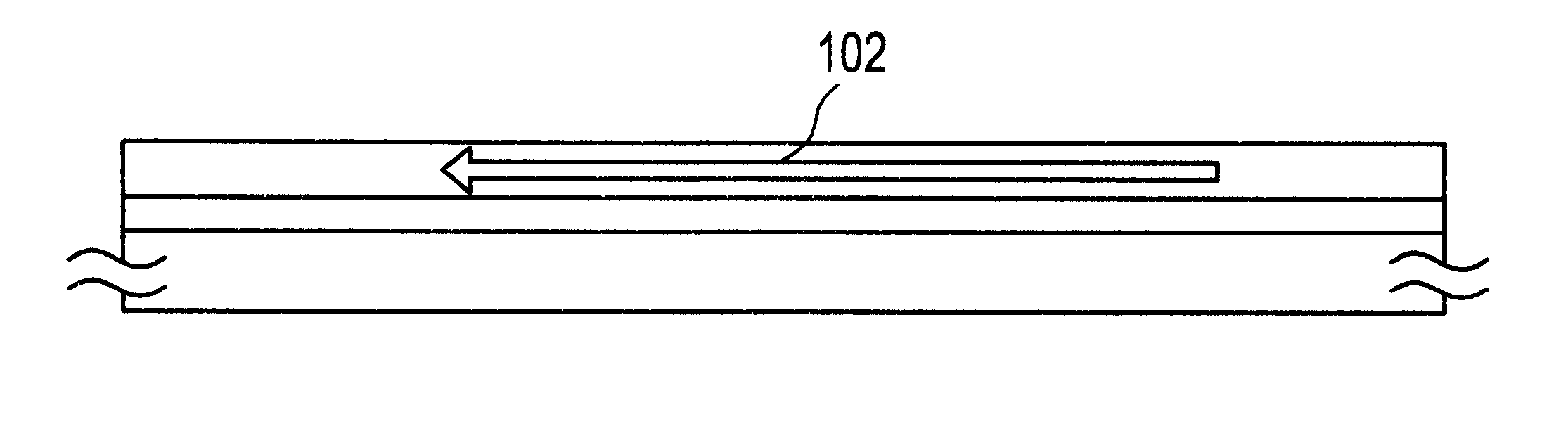
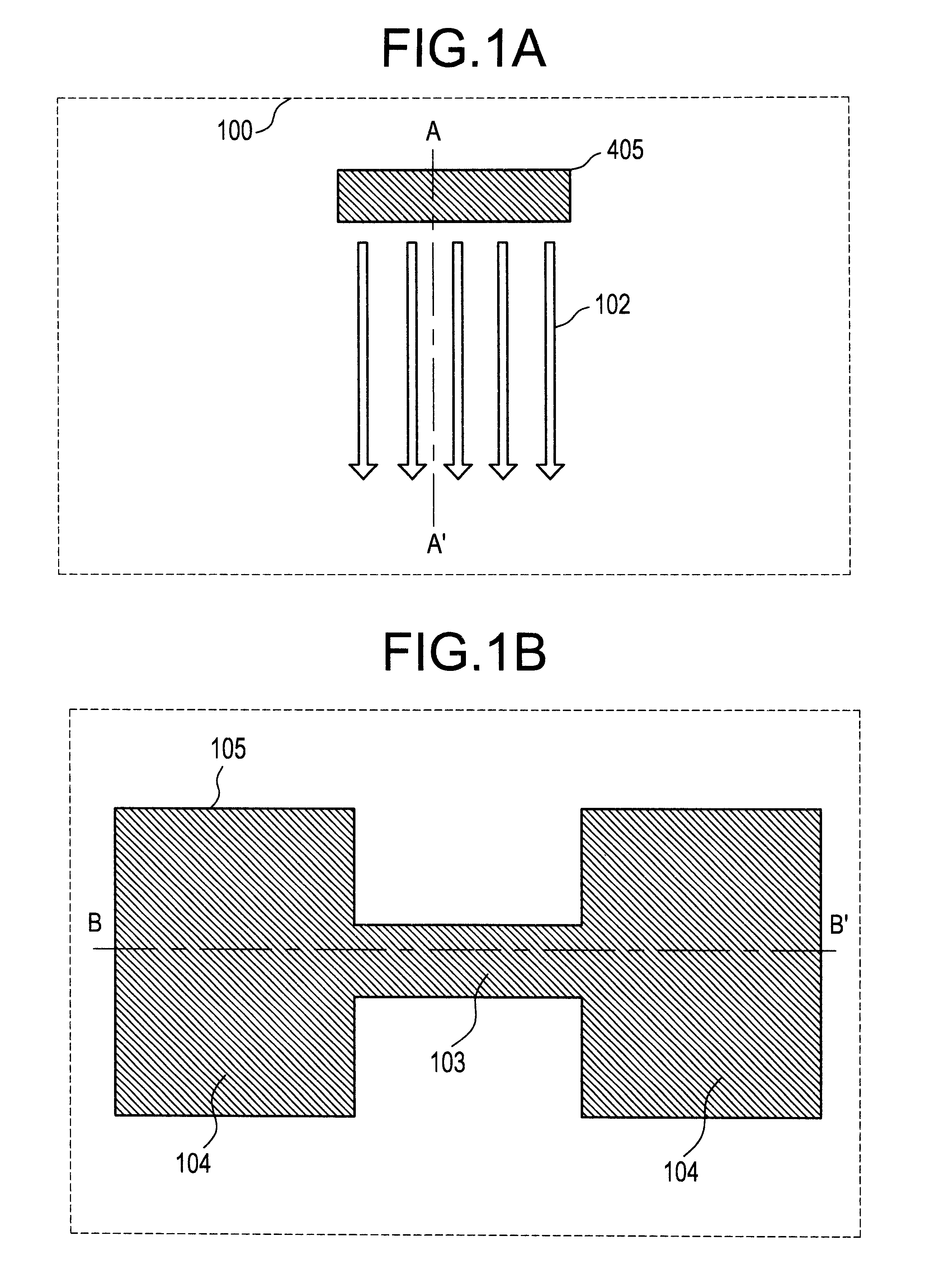
FIGS. 6A and 6B shows a part of the method for producing a TFT. In FIG. 6A, nickel element is introduced into a hatched region 601. Nickel element can be introduced in a manner similar to that employed in Example 1. However, it is necess...

example 4

In the present example, nickel element is introduced not selectively, but over the entire surface of the amorphous silicon film. Thus, in the processes shown in FIG. 1A and in FIG. 4A, a nickel acetate solution may be applied to the whole surface of the amorphous silicon film 403 without forming any masks (as shown by 404 in FIG. 4A)

When the example is employed, nickel is provided at the same concentration in the entire pattern region 105 in FIG. 1B or FIG. 4C. Accordingly, a diffusion of nickel which occurs from the region containing nickel at a high concentration to that containing no nickel (more precisely, a region containing nickel at a concentration below the detection limit or at an extremely low concentration) cannot be expected in this case.

However, after implanting impurity ions for the formation of source / drain regions as shown in FIG. 2A, since the regions other than the region 202 which becomes the channel forming region are rendered amorphous, if heating treatment perf...


PUM

PropertyMeasurementUnit
temperatureaaaaaaaaaa
heat resistanceaaaaaaaaaa

Abstract

The solution (for example, a nickel acetate solution) containing a metal element such as nickel which accelerates the crystallization of silicon is applied to an amorphous silicon film by spin coating using a mask, to retain nickel in contact with the surface of the amorphous silicon film. Then, heating treatment is performed to crystallize selectively the amorphous silicon film, so that an amorphous region and a crystalline region are formed in the silicon film. In this state, the silicon film is heated to diffuse the metal element from the crystalline region to the amorphous region, thereby decreasing a concentration of the metal element in the crystalline region.

Description

1. Field of the InventionThe present invention relates to a thin film transistor and a method for producing the same.2. Description of the Related ArtRecently, much attention is paid on a liquid crystal device with a constitution comprising thin film transistors (TFTs). In a device of this type denoted as an active matrix type liquid crystal display device, a TFT is formed in each of several million pixels or more arranged in matrix and the charge stored in each pixel is controlled by the TFT. Since a liquid crystal display device of the active matrix type enables a fine display at a high speed, it is utilized in a display device of a hand-held word processor or a computer.Generally, at present, in an active matrix type liquid crystal display device, the TFTs provided in each pixel is produced using an amorphous silicon film formed by plasma CVD, and a peripheral driver circuit for driving the TFTs provided to each pixel is constructed by an external IC. The peripheral driver circui...

Claims


Application Information

Patent Timeline
Patent Type & Authority Patents(United States)
IPC IPC(8): H01L21/02H01L21/336H01L21/20H01L21/322
CPCH01L21/2022H01L21/3221H01L29/66757H01L21/02488H01L21/02422H01L21/02532H01L21/02672
Inventor YAMAZAKI, SHUNPEIOHTANI, HISASHIMIYANAGA, AKIHARUTERAMOTO, SATOSHI
Owner SEMICON ENERGY LAB CO LTD
Why Eureka
Try Eureka