Semiconductor integrated circuit device

a technology of integrated circuits and semiconductors, applied in the direction of memory adressing/allocation/relocation, digital storage, instruments, etc., can solve the problems of limited number of circuits which can be installed, insufficient to meet the higher speed of mpu, and operation of data transfer

Inactive Publication Date: 2001-11-27
RENESAS ELECTRONICS CORP
View PDF14 Cites 30 Cited by
  • Summary
  • Abstract
  • Description
  • Claims
  • Application Information

AI Technical Summary

Problems solved by technology

However this is found to be insufficient to meet the higher speed of the MPU, and the main trend is for a system where a high speed memory is mounted as an auxiliary storage portion between the MPU and the main storage portion.
In these prior arts, there are problems such as a delay in the operation of the data transfer at the time of a cache mis hit, and hence an improved technology is proposed.
However, in the above-mentioned conventional technology, the occupied area of the two way transfer gate circuit becomes large so that the number of circuits which can be installed is limited.
As a result the number of transfer bus lines is also limited.
Furthermore, recently, there is a problem of a drop in the cache hit ratio for the case where an access request is received from a pl

Method used


Image

  • Semiconductor integrated circuit device
  • Semiconductor integrated circuit device
  • Semiconductor integrated circuit device

Examples


Embodiment Construction

of each Block

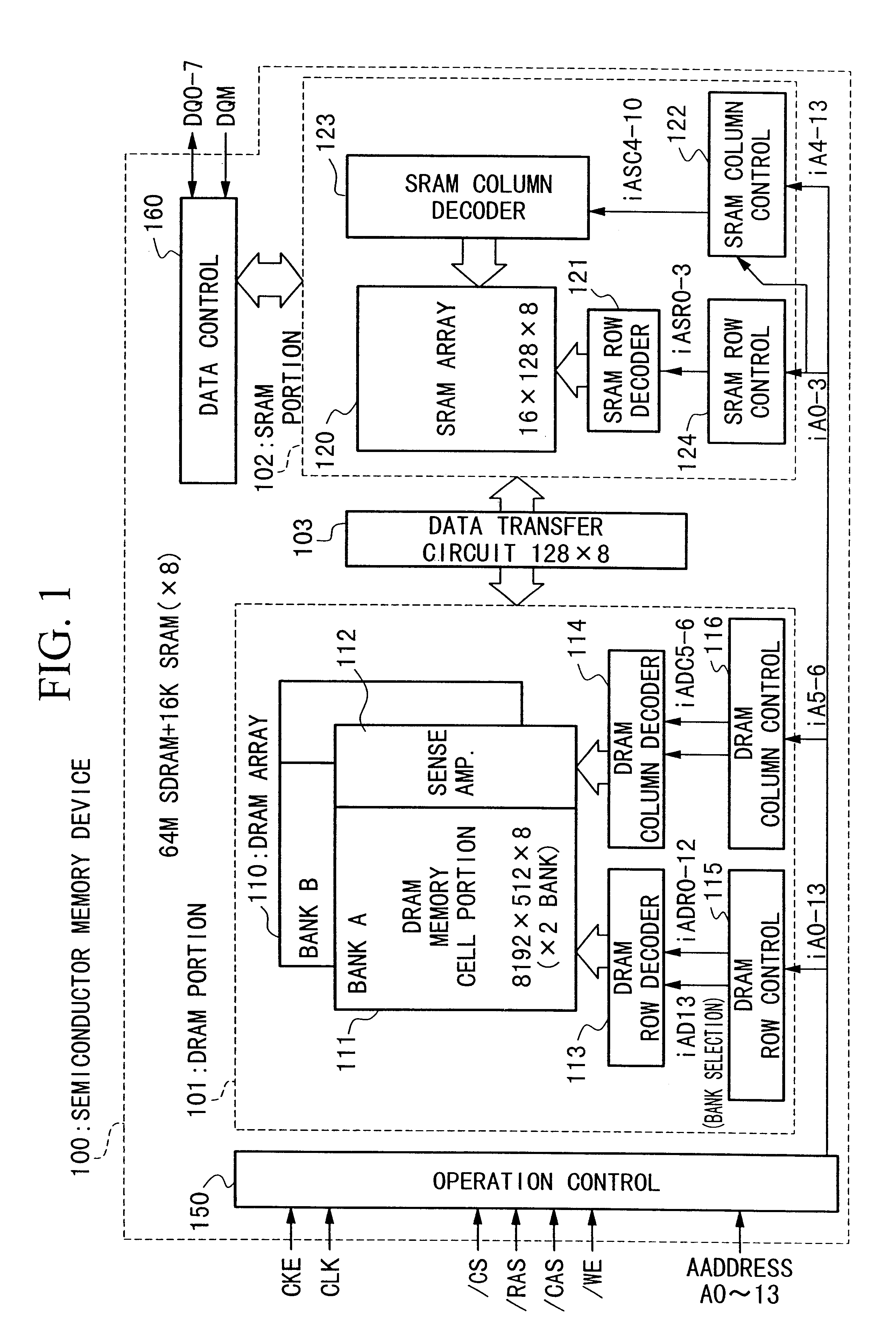
A detailed description will now be given of each circuit block of the overall block diagram shown in FIG. 1.

The following description strictly shows one embodiment, however the invention is not limited to this description.

1. "Operation Control Device"

FIG. 39 shows a block diagram of the operation control device. The operation control device 150 comprises; an internal clock generator 410, a command decoder 420, a control logic 430, an address control device 440, and a mode register 450. The internal clock generator 410 generates an internal clock signal iCLK from external input signals CLK and CKE. The internal clock signal iCLK is input to the command decoder 420, the control logic 430, the address control device 440, and a data control device, and performs timing control of each part.

The command decoder 420 has a buffer 421 for receiving respective input signals, and a command judgment circuit 422. The / CS signal, / RAS signal, / CAS signal, / WE signal and address signal...


PUM


Abstract

A semiconductor integrated circuit device which can save defect bits in an auxiliary storage portion functioning as a cache memory is provided. A redundant SRAM cell array MAR is provided so as to be adjacent to a SRAM cell array MA of a SRAM portion functioning as a cache memory, and with the positions of rows matching. Redundant cells which are alternatively selected based on redundant selection signals, are arranged in matrix form in this redundant SRAM cell array MAR. Moreover, a data input/output line SIOR is provided in each row of this SRAM cell array MAR, and each data input/output line SIOR is connected to a global data input/output line GIOR via a data input/output line connection circuit which is alternatively conduction controlled based on a predetermined selection signal. This global data input/output line GIOR is connected to a read/write bus line together with a read/write amplifier which is used at normal times.

Description

1. Field of the InventionThe present invention relates to a semiconductor integrated circuit device, namely a semiconductor integrated circuit device which has a main storage portion, and an auxiliary storage portion functioning as a cache memory, formed on the same semiconductor substrate, and a data transfer circuit between the main storage portion and the auxiliary storage portion. In particular the invention relates to a redundant configuration for saving defects of the auxiliary storage portion.2. Description of the Related ArtIn general, a relatively low speed low cost and large capacity semiconductor device is used as the main storage device used in a computer system. As a device which meets these requirements, a general purpose DRAM is generally used.Moreover, with recent computer systems speeding up of the DRAM constituting the main storage portion has resulted to meet the higher speed of systems (in particular the higher speed of the MPU). However this is found to be insuf...

Claims


Application Information

Patent Timeline
IPC IPC(8): G06F12/08G11C29/00G11C11/413G11C11/401G11C11/407G11C11/41G11C14/00G11C29/04
CPCG06F12/0893G11C14/00G11C29/846G06F2212/3042G11C29/00
Inventor MATSUI, YOSHINORI
Owner RENESAS ELECTRONICS CORP
Why Eureka
Try Eureka