Optimized alternating phase shifted mask design

a mask design and alternating phase technology, applied in the field of very large scale integrated circuit devices, can solve the problems of affecting the layout density of the layout, the inability to print images by residual phase edges, and the limited resolution of the exposure system

Inactive Publication Date: 2002-01-15
IBM CORP
View PDF6 Cites 129 Cited by
  • Summary
  • Abstract
  • Description
  • Claims
  • Application Information

AI Technical Summary

Benefits of technology

is to provide a method of altPSM lithography which can overcome the problems associated with lens abe

Problems solved by technology

The resolution of an exposure system is limited by the contrast of the projected image, that is, the intensity difference between adjacent light and dark features.
The challenge that needs to be met before introducing hard phase shifters to VLSI product programs lies in the rapid, reliable design modifications of complex chip designs.
A major issue in the imaging of bright field layouts, i.e. layouts that seek to print dark line patterns in a clear background, with altPSM is the fact that the altPSM design and manufacturing process forces closed loop topologies on the phase shapes.
The same de

Method used


Image

  • Optimized alternating phase shifted mask design
  • Optimized alternating phase shifted mask design
  • Optimized alternating phase shifted mask design

Examples


Embodiment Construction

)

In describing the preferred embodiment of the present invention, reference will be made herein to FIGS. 1-11 of the drawings in which like numerals refer to like features of the invention. Features of the invention are not necessarily shown to scale in the drawings.

The present invention provides a simple and novel method of reducing the undesirable effects of lens aberrations and proximity effects during the photolithography process of a desired mask pattern using multiple and uniform phase shifted regions to define the line regions of the desired mask pattern. Manufacturers may practice the method of the present invention with currently installed tool sets and equipment.

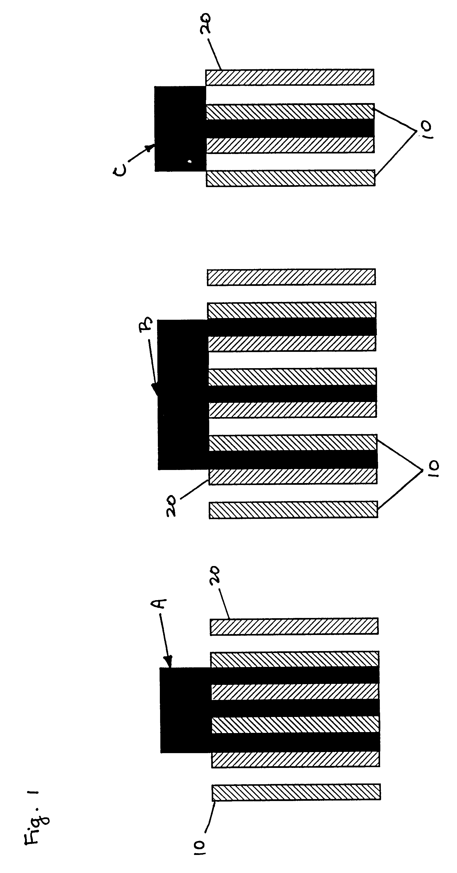
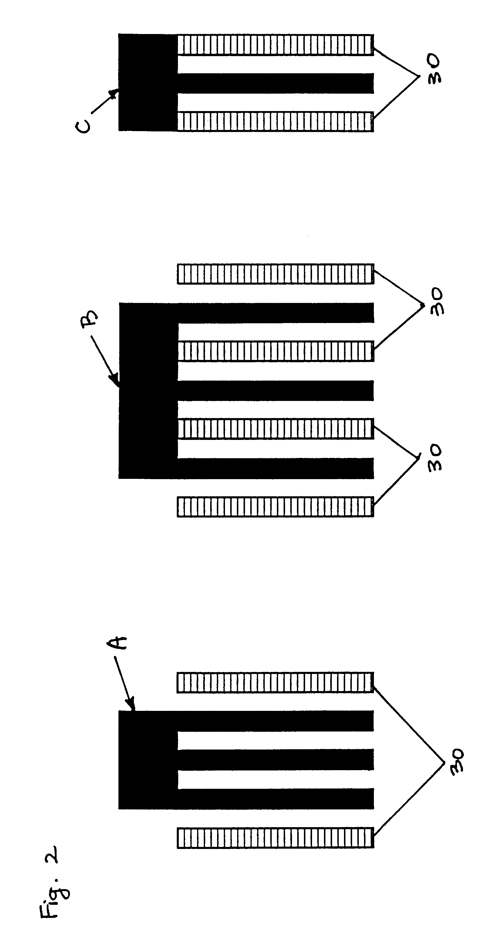
In FIG. 1 is shown an enhanced phase shifted mask layout having features or line regions A, B and C illustrated in solid black lines wherein line region A is most nested and line region C comprises a single isolated line. On either side of each single line (shown here as vertical, solid black lines) are alternating...


PUM


Abstract

A method for reducing lens aberrations sensitivity and proximity effects of alternating phase shifted masks is described. The critical features of a chip design layout are first identified. Multiple, narrow phase regions and auxiliary phase transitions, which provide additional opaque features, are then formed alongside the critical features such that a grating pattern of substantially uniform pitch is printed. Together with a complementary trim mask, the circuit pattern so delineated has reduced sensitivity to lens aberrations and proximity effects.

Description

1. Field of the InventionThe present invention relates to the manufacture of very large scale integrated (VLSI) circuit devices. In particular, the present invention provides a method and apparatus for converting a chip design into a phase shifted mask design for producing the chip.2. Description of Related ArtA very large scale integrated (VLSI) complementary metal oxide semiconductor (CMOS) chip is manufactured on a silicon wafer by a sequence of material additions (i.e., low pressure chemical vapor depositions, sputtering operations, etc.), material removals (i.e., wet etches, reactive ion etches, etc.), and material modifications (i.e., oxidations, ion implants, etc.). These physical and chemical operations interact with the entire wafer. For example, if a wafer is placed into an acid bath, the entire surface of the wafer will be etched away. In order to build very small electrically active devices on the wafer, the impact of these operations has to be confined to small, well de...

Claims


Application Information

Patent Timeline
IPC IPC(8): G03F7/20G03F1/00
CPCG03F7/70425G03F1/30
Inventor LIEBMANN, LARS W.WONG, ALFRED K.
Owner IBM CORP
Why Eureka
Try Eureka