

Self-aligned clock recovery circuit with proportional phase detector
a clock recovery circuit and phase detector technology, applied in the direction of instruments, digital transmission, generating/distributing signals, etc., can solve the problems of reducing the allowable bandwidth of optical signals, fiber span, and jitter reduction
- Summary
- Abstract
- Description
- Claims
- Application Information
AI Technical Summary
Benefits of technology
Problems solved by technology
Method used
Image

Examples
Embodiment Construction
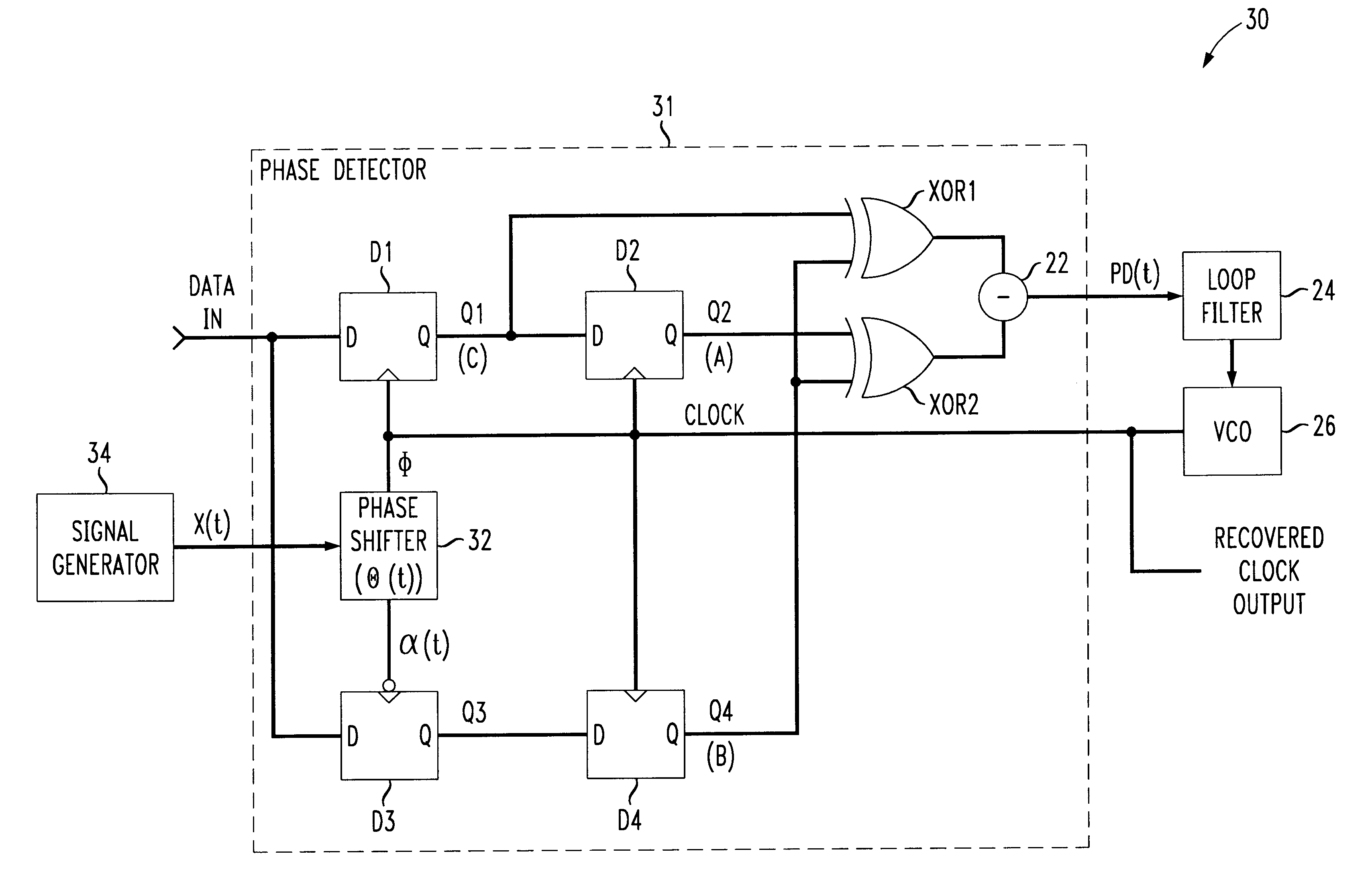
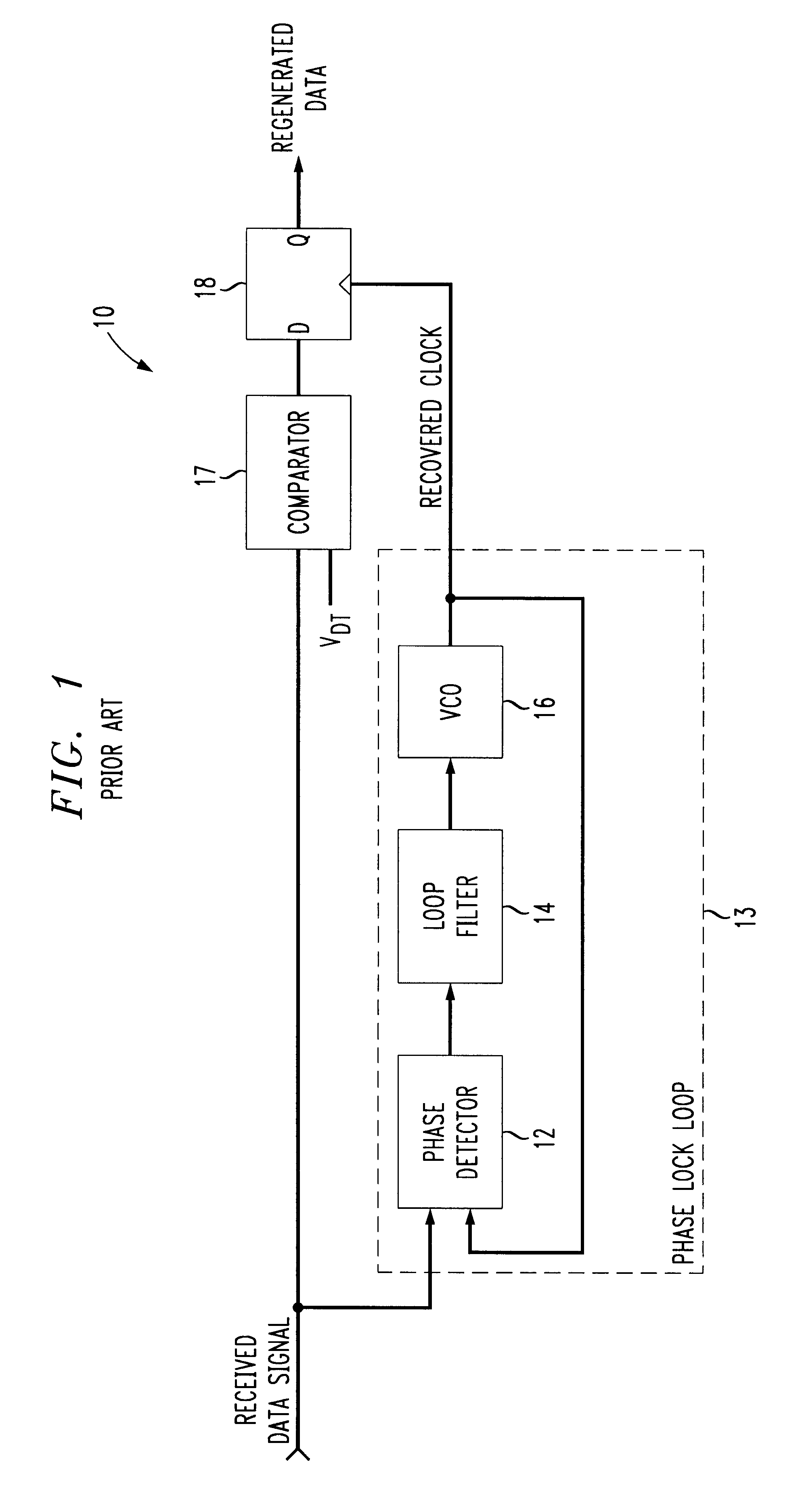
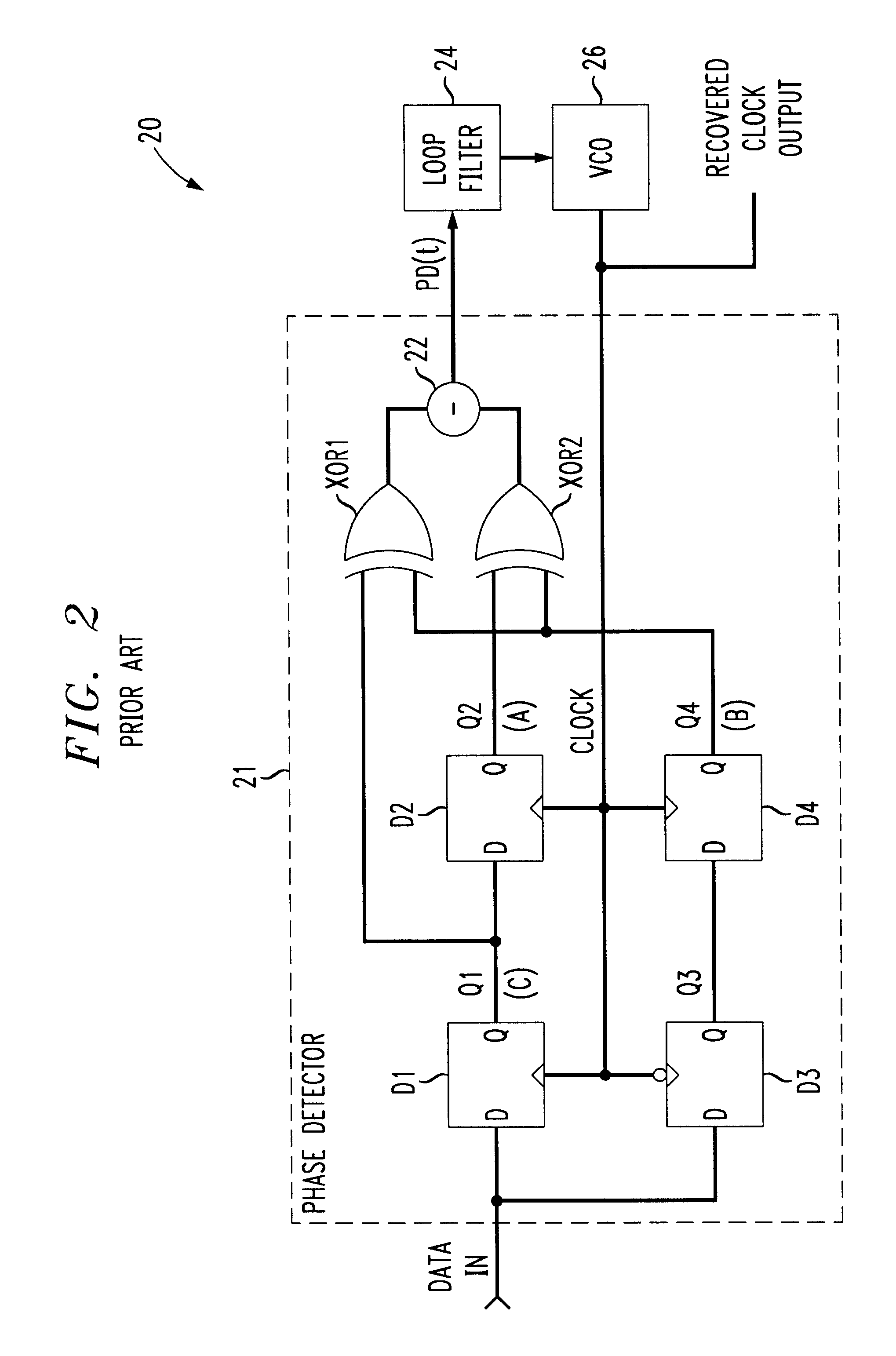
To provide a foundation for the teachings of the present invention, the operation of a prior art clock recovery circuit based on a sampling phase detector will first be discussed in detail. An illustrative embodiment of the invention to be described represents an improvement upon this prior art circuit.
Referring now to FIG. 2, prior art clock recovery circuit 20 includes a sampling phase detector 21 that receives an input data signal, a loop filter 24 and a VCO 26 (local clock generator) which provides a recovered clock output based on the input data signal. Clock recovery circuit 20 functions to synchronize the VCO clock output with the symbol to symbol timing of the input data signal. Phase detector 21 is comprised of four sampling circuits D1-D4, a pair of exclusive OR gates XOR1, XOR2 and a subtracter 22 which subtracts the output of XOR1 from XOR2. Phase detector 21 is known as the Alexander phase detector and is widely used in present day high speed clock recovery circuits. Th...
PUM
 Abstract
Description
Claims
Application Information