Input buffer circuit for low power application

a low-power application and input buffer technology, applied in logic circuit coupling/interface arrangement, pulse technique, instruments, etc., can solve the problems of high power dissipation used in memory applications, possibility of multiple transitions, and high power use than necessary

Inactive Publication Date: 2002-04-02
ETRON TECH INC
View PDF6 Cites 7 Cited by
  • Summary
  • Abstract
  • Description
  • Claims
  • Application Information

AI Technical Summary

Problems solved by technology

Buffer circuits are an integral element in many memory-oriented applications; however, previous applications of the buffer circuits have often resulted in higher power use than necessary.
One of the problems with the prior art is the high power dissipa

Method used


Image

  • Input buffer circuit for low power application
  • Input buffer circuit for low power application
  • Input buffer circuit for low power application

Examples


Embodiment Construction

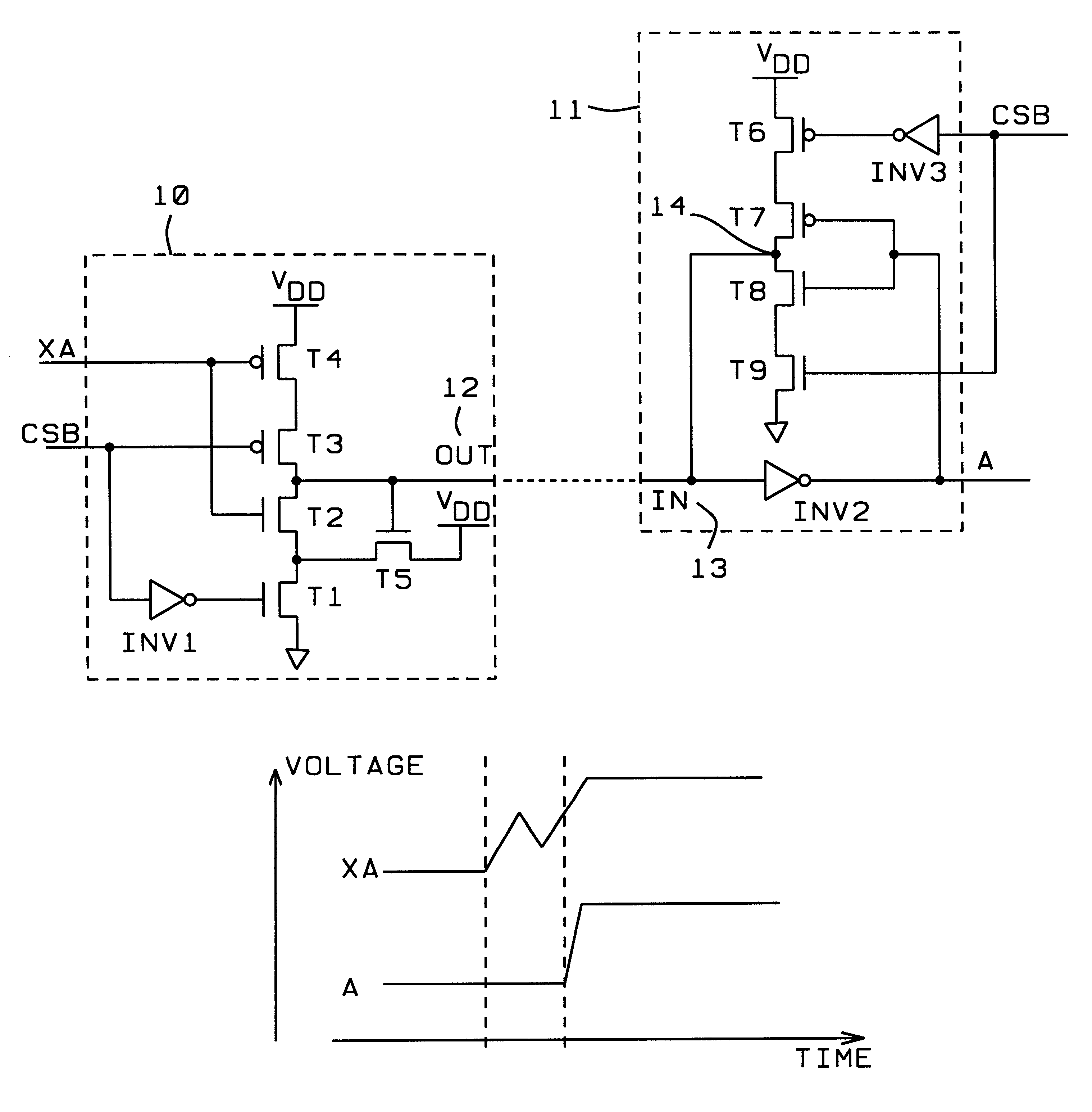
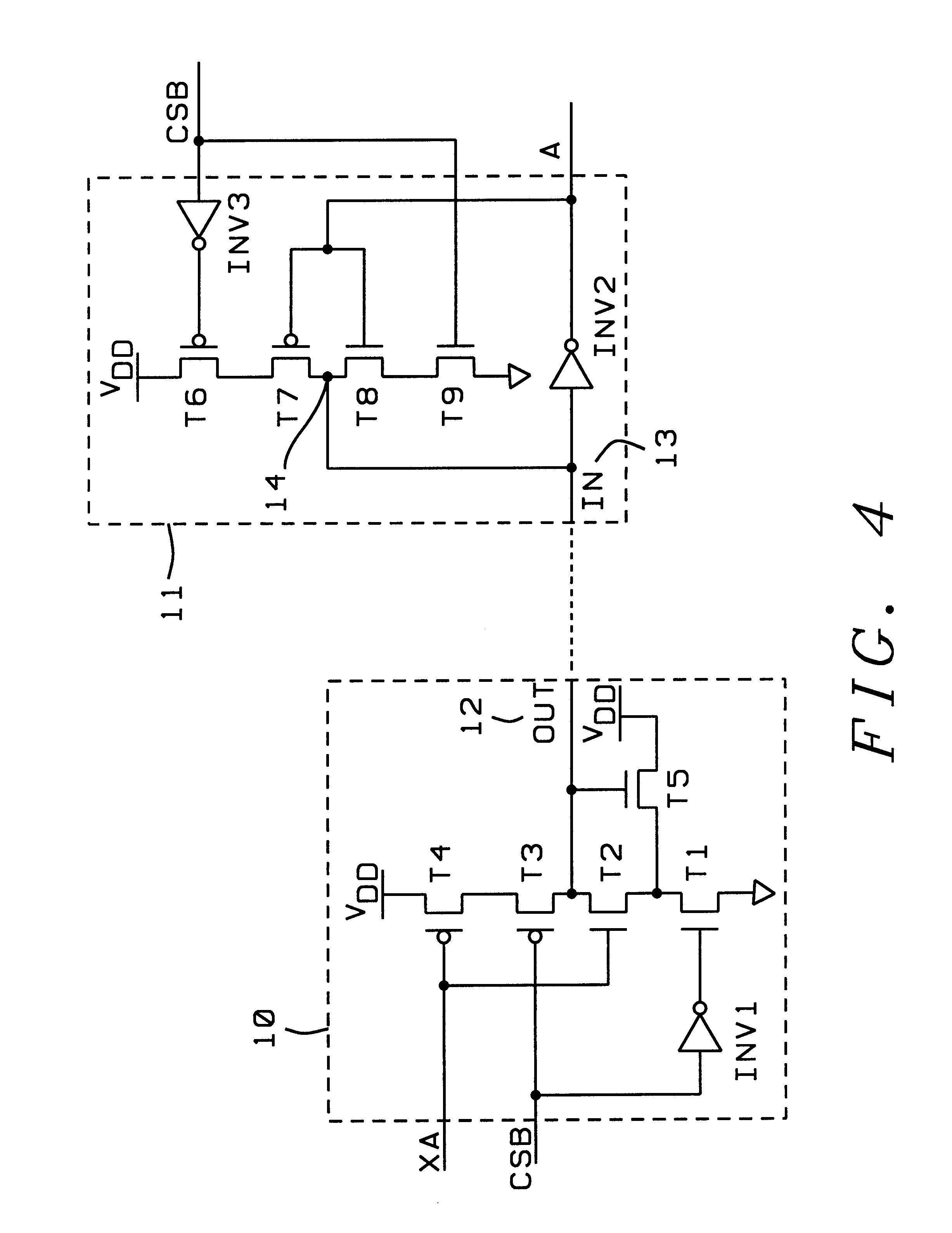
12 is the inverse of XA when CSB=0, and when CSB=0 and XA=1, then OUT=0.

Continuing to refer to FIGS. 4 and 7, consider the case where CSB=0 and XA=0. The value of CSB is inverted by Inverter INV1, so that a "1" appears at the Gate of nFET T1. The "1" level at the Gate makes nFET T1 active, and current may flow. CSB directly feeds the pFET T3 with a "0" level, making T3 active. Since XA=0, the Gate of nFET T2 is biased to make T2 inactive. However, XA feeds the Gate of the pFET T4 with a 0 level causing T4 to be active. The OUT signal 12 from the Schmitt Trigger is thus determined by nFET T5, which is inactive because the current from V.sub.DD passes through the active T4 and T3. Thus, OUT 12 is at the "1" level. The Gate of T5 will stabilize at "1" confirming that T5 is inactive. Again, for all XA, OUT is the inverse of XA when CSB=0. In this case OUT=1.

Continue to refer to FIGS. 4 and 7, when CSB=1, the OUT line 12 of the Schmitt trigger is placed in a high Z state, and the value o...


PUM


Abstract

An input buffer receiver is described that will latch on a particular transition to insure a single transition does not have multiple transitions due to disturbances. This is accomplished with a Schmitt Trigger and a feedback latch controlled by an enabling signal. In one application, this is a chip select. A chip addressing input to a Schmitt Trigger type tri-state buffer is applied in parallel to two gates of the plurality of stacked CMOS transistors. A chip selection (CSB) signal is applied to a first gate of the Schmitt Trigger type tri-state buffer and in parallel to a second gate through an inverter. The output of the tri-state buffer is then fed to a latch circuit comprised of a plurality of stacked CMOS transistors. The latch output is the signal that goes to the circuitry that selects the desired chip address. The latch output is fed back into the appropriate gates of the latch to effect the desired latch-up when the Schmitt Trigger is put into the high output impedance state. The latchup during this hi-Z state prevents the latch output from changing whenever the chip addressing input to the Schmitt Trigger changes due to circuit disturbances. The latchup also prevents reconfiguration of down stream circuitry when selection is not done, thus minimizing the use of power. The tri-state capability uses an hysteresis effect to produce higher trip points when the Schmitt Trigger is not in the hi-Z mode and the input switches low, and lower trip points when the trigger switches high thus eliminating unwanted circuit noise effects.

Description

1. Field of InventionThe present invention relates in general to complementary MOS (CMOS) circuits to provide low power buffer capability, and more particularly to a CMOS Schmitt trigger with a tri-state feature and a latching circuit.2. Description of Related ArtBuffer circuits are an integral element in many memory-oriented applications; however, previous applications of the buffer circuits have often resulted in higher power use than necessary. In addition, the previous applications have been subject to multiple transitions of state, when only one transition is desired.U.S. Pat. No. 3,984,703 (Jorgensen) describes a classic CMOS Schmitt trigger circuit of the prior art. Jorgensen describes an improvement that addresses both high power drain and uneconomical use of die space.U.S. Pat. No. 5,450,019 (McClure, et al.) describes the use of Schmitt triggers to control a precharge circuit to terminate when the output terminal has reached an intermediate voltage, so that oscillations ar...

Claims


Application Information

Patent Timeline
IPC IPC(8): H03K3/3565H03K3/00H03K5/1252H03K5/125H03K3/356
CPCH03K3/356121H03K5/1252H03K3/3565
Inventor LIU, SHI HUEISHIH, JENG TZONG
Owner ETRON TECH INC
Why Eureka
Try Eureka