

Organic electroluminescent device with high resistance inorganic hole injecting layer
a technology of electroluminescent devices and inorganic holes, which is applied in the direction of discharge tubes/lamp details, discharge tubes luminescnet screens, electric discharge lamps, etc., can solve the problems of difficult to achieve effective recombination in the light emitting layer, and achieve excellent hole injection efficiency, low operating voltage, and improved luminous efficiency
- Summary
- Abstract
- Description
- Claims
- Application Information
AI Technical Summary
Benefits of technology
Problems solved by technology
Method used
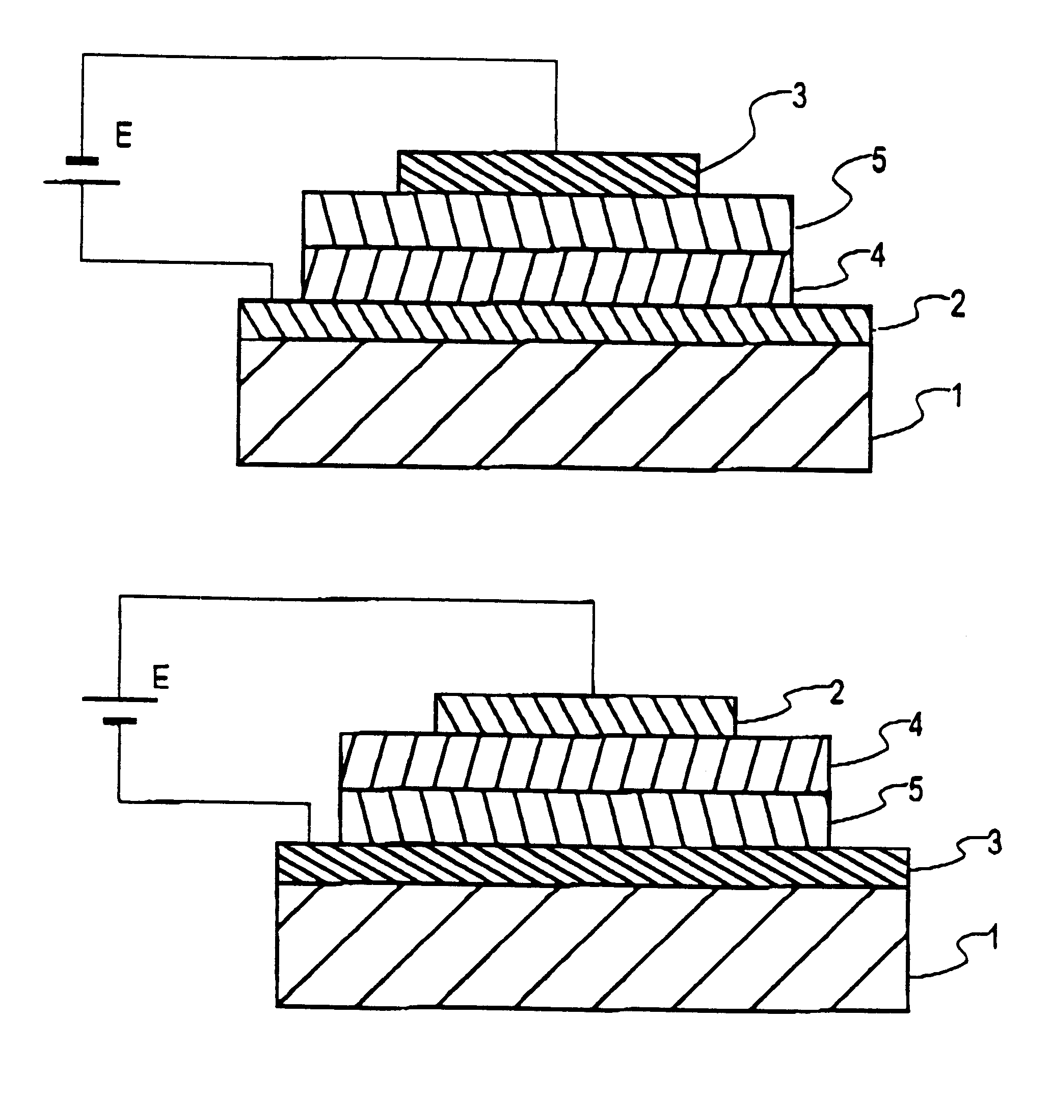
Image

Examples
example 1
A substrate of (7059) glass by Corning Glass Works was scrubbed using a neutral detergent.
By RF magnetron sputtering from a target of ITO oxide, a hole injecting electrode layer of ITO having a thickness of 200 nm was formed on the substrate at a temperature of 250.degree. C.
After its ITO electrode-bearing surface was cleaned with UV / O.sub.3, the substrate was secured by a holder in a sputtering chamber, which was evacuated to a vacuum of 1.times.10.sup.-4 Pa or lower.
Next, using a target of SiO.sub.2 having a gold pellet of a predetermined size rested thereon, a high resistance inorganic hole injecting layer was deposited to a thickness of 20 nm. The sputtering gas used was a mixture of 30 sccm of Ar and 5 sccm of O.sub.2. Sputtering conditions included room temperature (25.degree. C.), a deposition rate of 1 nm / min, an operating pressure of 0.2 to 2 Pa, and an input power of 500 W. The inorganic hole injecting layer as deposited had a composition of SiO.sub.1.9 containing 4 mol % ...
example 2
In the step of depositing the high resistance inorganic hole injecting layer in Example 1, a target of GeO.sub.2 having a gold pellet of a predetermined size rested thereon was used. The high resistance inorganic hole injecting layer was deposited to a thickness of 20 nm. The sputtering gas used was a mixture of 30 sccm of Ar and 5 sccm of O.sub.2. Sputtering conditions included room temperature (25.degree. C.), a deposition rate of 1 nm / min, an operating pressure of 0.2 to 2 Pa, and an input power of 500 W. The inorganic hole injecting layer as deposited had a composition of GeO.sub.2 containing 2 mol % of Au.
Otherwise as in Example 1, an organic EL device was obtained. The organic EL device was driven in air at a constant current density of 10 mA / cm.sup.2, finding an initial luminance of 900 cd / m.sup.2 and a drive voltage of 7 volts.
The sheet resistance of the high resistance inorganic hole injecting layer was measured by the four-terminal method. The layer having a thickness of 1...
example 3
Organic EL devices were fabricated as in Example 1 except that in the step of depositing the inorganic insulative hole injecting layer in Examples 1 and 2, the flow rate of O.sub.2 in the sputtering gas was changed and the target used was changed in accordance with the desired layer composition so that the resulting layers had the compositions SiO.sub.1.7, SiO.sub.1.95, GeO.sub.1.96, and Si.sub.0.5 Ge.sub.0.5 O.sub.1.92, respectively. The devices were tested for emission luminance, obtaining substantially equivalent results.
PUM
 Abstract
Description
Claims
Application Information