Motion circuit and on-board driver circuit for liquid crystal display panel employing the motion circuit

a technology of motion circuit and driver circuit, which is applied in the direction of static storage, digital storage, instruments, etc., can solve the problems of driver circuit malfunction, driver circuit failure, and poor performance of polycrystalline silicon in the speed of transmitting clock signals to the driver circuit, so as to reduce the occurrence of failure phenomenon and ensure stable circuit operation without malfunction

Inactive Publication Date: 2002-04-16
TOSHIBA MATSUSHITA DISPLAY TECH
View PDF2 Cites 37 Cited by
  • Summary
  • Abstract
  • Description
  • Claims
  • Application Information

AI Technical Summary

Benefits of technology

is to provide a motion circuit which reduces the occurrence of the fail phenomenon due to the skew between a normal phase and a reverse phase clock signal for driving shift registers, thereby performing stable circuit operations with no malfunctions.

Problems solved by technology

However, polycrystalline silicon is inferior to single crystalline silicon in the speed of transmitting clock signals to the driver circuits, so a normal phase and a reverse phase clock signal have to be entered instead of a single phase clock signal.
In contrast, the use of polycrystalline silicon causes a longer delay time in the inverters, so that the generation of the normal phase and the reverse phase clock signal from the single clock signal might cause malfunctions of the driver circuit due to the skew between the normal phase and the reverse phase clock signal.
In other words, a large skew between the normal phase and the reverse phase clock signal causes a so called fail phenomenon according to which the shift registers cannot latch signals at each stage sent from a previous stage, which prevents signals normally shifted in time from being outputted from the shift registers.
As a result, the driver circuit causes malfunctions.
In the on-board driver circuit shown in FIG. 25, supplying a normal phase and a reverse phase clock signal from the external circuit 41 requires two clock signal lines for each of the scanning side driver circuit 42 and the image signal side driver circuit 43, so that a total of four clock signal lines are needed for external connection, which causes troublesome connecting operations.
In the on-board driver circuit composed of polycrystalline silicon semiconductor layers shown in FIG. 26, on the other hand, the characteristics of the thin-film transistors are far poorer than a driver circuit composed of single crystalline silicon, so that the power-supply voltage must be set at a higher level than in a MOSFET integrated circuit with single crystalline silicon.
Thus, the fail phenomenon is caused when two-phase clock signals are entered, the same as when a single phase clock signal is entered, which makes it impossible to secure stable circuit operations of the shift registers.
In order to realize a smaller and thinner liquid crystal display panel, it has been considered to built a timing circuit on the same board as other units; however, it is impossible unless the fail phenomenon due to a clock skew is solved.
These problems are common to all motion circuits which are composed of polycrystalline silicon semiconductor layers and which have shift registers shifting start signals in time with a normal phase and a reverse phase clock signal.
Even if the input potential of the second inverter increases, it fails to reach the threshold of the second inverter in a skew period because the delay circuit provided between each adjacent stages of the shift register delays the input voltage starting to change.
When a normal phase and reverse phase clock signals are generated from an entered single phase clock signal with a driver circuit composed of a polycrystalline silicon semiconductor, the inverters have a delay time to generate the reverse phase clock signal, causing a clock skew of several tens of nanoseconds.
This does not secure stable operations of the shift register.

Method used


Image

  • Motion circuit and on-board driver circuit for liquid crystal display panel employing the motion circuit
  • Motion circuit and on-board driver circuit for liquid crystal display panel employing the motion circuit
  • Motion circuit and on-board driver circuit for liquid crystal display panel employing the motion circuit

Examples


embodiment 2

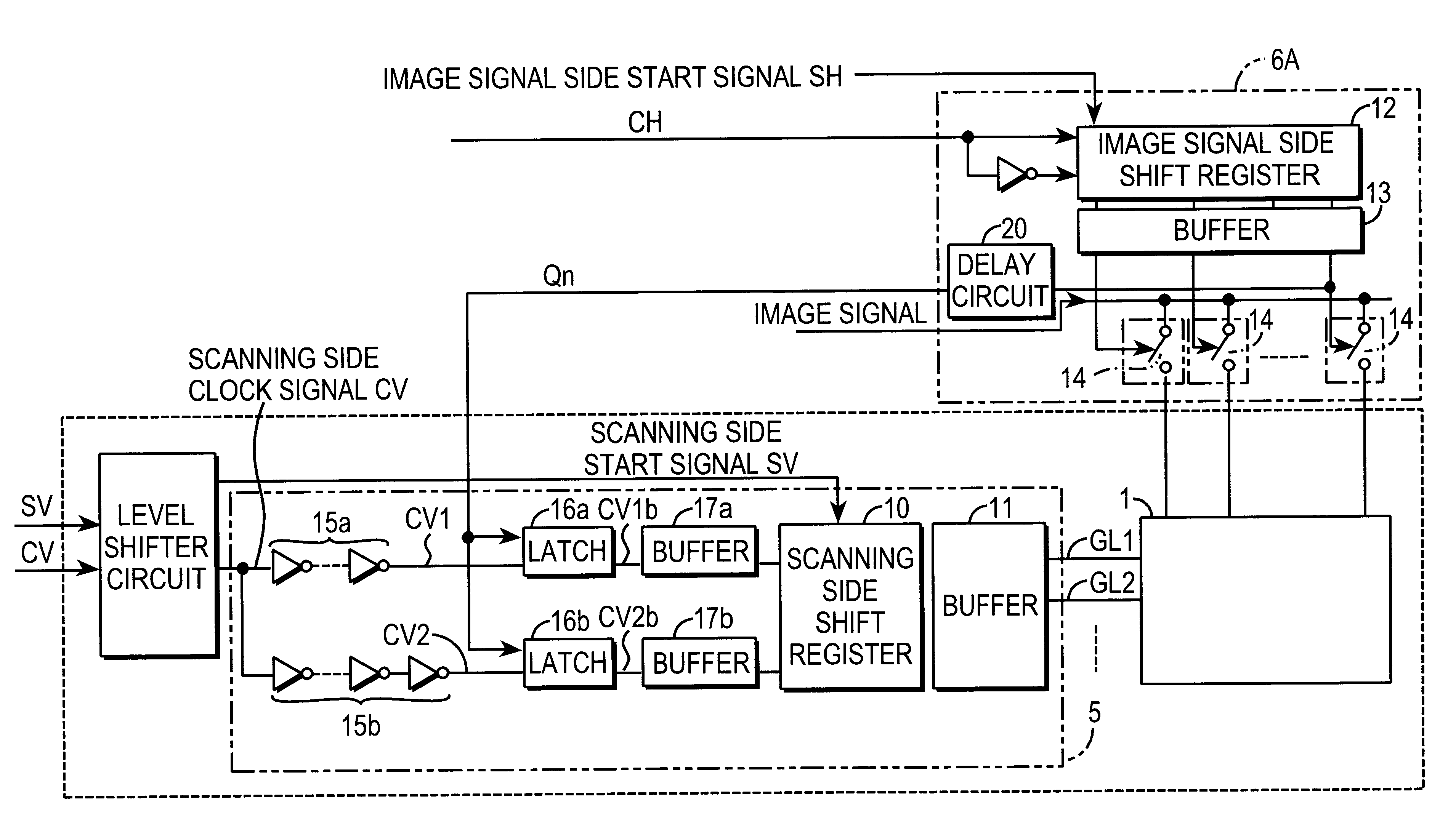
FIG. 9 is a diagram showing the entire structure of the driver circuit of Embodiment 2, and FIGS. 10(a)-10(f) are the timing charts of the driver circuit. In the present embodiment, the scanning side driver circuit 5 is a circuit internal to a liquid crystal display panel, but an image signal side driver circuit 6A, which is composed of single crystalline silicon, is an external circuit. The image signal side driver circuit 6A is external because it must be composed of single crystalline silicon transistors to meet the demands for high transistor performance when a liquid crystal display panel has a large screen. Consequently, in the present embodiment, the image signal side clock signal has a much shorter period than that in Embodiment 1, so that the skew period of a normal phase and reverse phase scanning side clock signals CV1 and CV2 becomes longer than that of the image signal side clock signal CH. This makes it impossible to use the image signal side clock signal CH as a latch...

embodiment 3

FIG. 13 is a diagram showing the structure of the main part of the driver circuit of Embodiment 3. The feature of the driver circuit of Embodiment 3 is that the normal phase and reverse phase clock signals CK1 and CK2 having no clock skew are generated from the single phase clock signal CK by using two inverter chain circuits. FIG. 13 shows a first inverter chain circuit 21, a second inverter chain circuit 22, and a shift register 23. The first and second inverter chain circuits 21 and 22 have different number of connected inverters from each other by one, so that their outputs are logical reverse to each other. The first inverter chain circuit 21 will enter the single phase clock signal CK and supply the normal phase clock signal CK1 to the shift register 23. The second inverter chain circuit 22 will enter the single phase clock signal CK and supply the reverse phase clock signal CK2 to the shift register 23.

The first and second inverter chain circuits 21 and 22 are structured as f...

embodiment 4

FIG. 15 is a diagram showing the structure of the main part of the driver circuit of Embodiment 4. The diagram shows an inverter 31, a delay circuit 32 having the same delay time as the inverter 31 and not performing logical reverse at its input / output terminals, buffers 33 and 34, and a shift register 35. The delay circuit 32 can be composed of a transfer gate or internal resistance (resistance of semiconductor layers composed of ion-doped polycrystalline silicon). In the structure, a reverse phase clock signal CK4, which is the reverse of a single phase clock CK, becomes the output of the inverter 31. A normal phase clock signal CK3 having the same phase as the single phase clock CK, on the other hand, becomes the output of the delay circuit 32. Since the delay circuit 32 has the same length of delay time as the inverter 31, there is no clock skew between the reverse phase clock signal CK4 and the normal phase clock signal CK3. As a result, the shift register 35 is supplied with t...


PUM

PropertyMeasurementUnit
timeaaaaaaaaaa
threshold voltageaaaaaaaaaa

Abstract

The motion circuit of the present invention is an on-board driver circuit which is composed of polycrystal silicon semiconductor layers formed on a substrate, and which is provided with a first latch circuit for latching one of a normal phase and reverse phase clock signals having a clock skew using a clock signal and for outputting it to a shift register, and a second latch circuit for latching the other one of the normal phase and reverse phase clock signals using a clock signal and for outputting to the shift register. The latch operations of the first and second latch circuits are timed to make the two clock signals have reverse polarities. Consequently, it is realized to provide a motion circuit performing stable circuit operations without malfunctions, by preventing the occurrence of the fail phenomenon due to a skew between the normal phase and reverse phase clock signals which drive the shift register. It is also realized to provide an on-board driver circuit for a liquid crystal display panel by employing the motion circuit.

Description

(1) Field of the InventionThe present invention relates to a motion circuit which is composed of polycrystalline silicon semiconductor layers and has a logical circuit performing established operations with a normal phase and a reverse phase clock signal, and more specifically, to a motion circuit comprising a shift register such as a transfer gate type shift register, which shifts an entered start signal in time with a normal phase and a reverse phase clock signal.The present invention also relates to an on-board driver circuit for a liquid crystal display panel employing the motion circuit.(2) Description of the Prior ArtDriver circuits displaying images on a matrix display panel have been required to perform higher-speed operations as the display panel has a larger screen and higher resolution. To meet the demands, a driver circuit unit is generally made of a high-speed single crystalline silicon LSI and connected to a display panel from outside.FIG. 25 is a circuit diagram showi...

Claims


Application Information

Patent Timeline
Patent Type & Authority Patents(United States)
IPC IPC(8): G09G3/36G11C19/28G11C19/00G09G5/18G02F1/133G09G3/20
CPCG09G3/3648G09G3/3677G11C19/28G09G3/3688G09G3/2011G09G5/18G09G2300/0408G09G2310/027G09G3/36
Inventor YAMAKURA, MAKOTOADACHI, KATSUMI
Owner TOSHIBA MATSUSHITA DISPLAY TECH
Why Eureka
Try Eureka