Method of forming a semiconductor thin film on a plastic substrate

a plastic substrate and semiconductor technology, applied in the direction of semiconductor devices, electrical equipment, transistors, etc., can solve the problems of deformation of the substrate, imperfect crystal thereby obtained, and partial damage of the amorphous silicon film,

Inactive Publication Date: 2002-04-23
SONY CORP
View PDF9 Cites 37 Cited by
  • Summary
  • Abstract
  • Description
  • Claims
  • Application Information

AI Technical Summary

Problems solved by technology

The amorphous silicon film may be thereby partially damaged.
However, the crystal thereby obtained is imperfect and not fully polycrystallized.
However, since a plastic substrate has low heat resistance, he...

Method used


Image

  • Method of forming a semiconductor thin film on a plastic substrate
  • Method of forming a semiconductor thin film on a plastic substrate
  • Method of forming a semiconductor thin film on a plastic substrate

Examples


Embodiment Construction

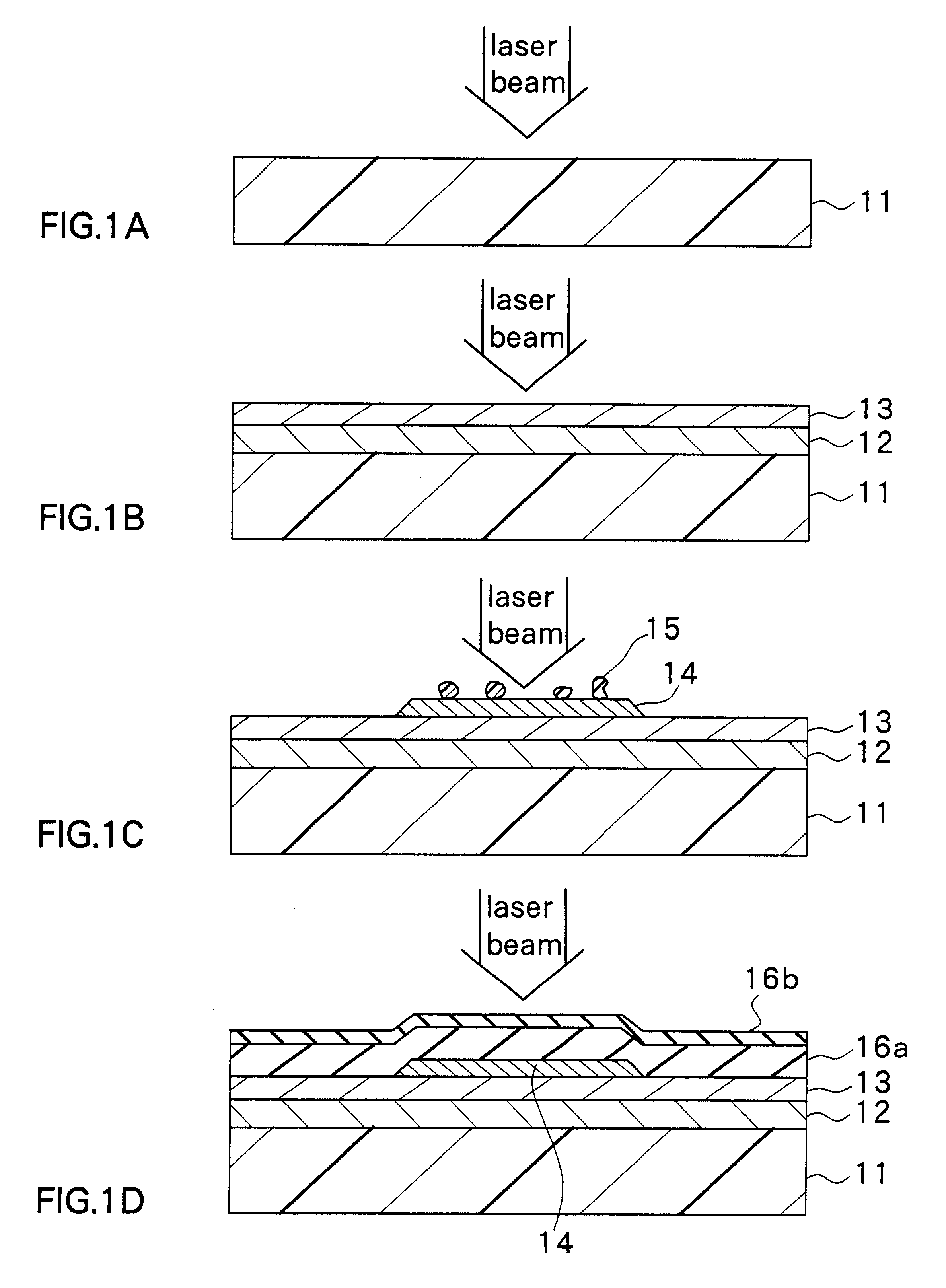
An example to which the method of forming a semiconductor thin film of the invention is applied will now be described.

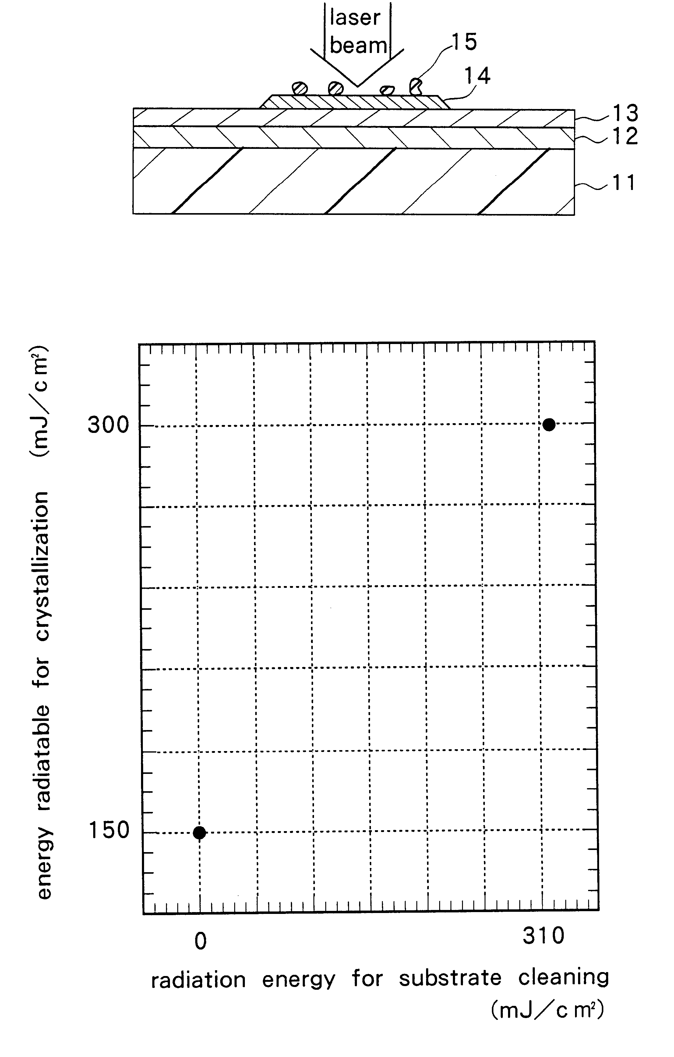
A quartz substrate was utilized in the example. The substrate was radiated with ten pulses of excimer laser beam whose energy (radiation energy for substrate cleaning) is approximately 310 mJ / cm.sup.2 for removing volatile contaminants deposited on surfaces of the substrate and a thin film formed on the substrate. On the substrate free of volatile contaminants, a plurality of amorphous silicon films having source and drain regions were provided through the method of forming a thin film transistor described in the foregoing embodiment. For the polycrystallization, the amorphous silicon films were radiated with 100 pulses of the excimer laser beam with a different energy intensity for each film.

The result was that the silicon film was not damaged with the laser beam energy (radiatable energy) of 300 mJ / cm.sup.2, as shown in FIG. 4. The energy value of 300 mJ / cm.sup.2 i...


PUM


Abstract

A method is provided for forming a semiconductor thin film which is free from damage to the film with radiation of a pulse laser beam with the optimum energy value for perfect polycrystallization. For forming an amorphous silicon thin film, a surface of a plastic substrate as a base and insulating layers are each radiated with a pulse laser beam for removing volatile contaminants like a resist as a pretreatment. Damage to the film caused by a gas emitted from the base substrate and the insulating layers resulting from volatile contaminants is thus prevented. A protective layer including a gas barrier layer and a refractory buffer layer is formed on the substrate. Gas penetration from the substrate to the amorphous silicon film is thereby prevented. Conduction of heat produced by energy beam radiation to the substrate is prevented as well. It is possible to increase energy intensity of energy beam radiated for polycrystallization of the amorphous silicon film to the optimal value for perfect polycrystallization.

Description

1. Field of the InventionThe present invention relates to a method of forming a semiconductor thin film including a process of cleaning a surface of semiconductor substrate or an insulating substrate made of glass, plastic and the like or a surface of thin film formed on such a substrate. In particular, the invention relates to a method of forming a semiconductor thin film wherein polycrystallization of amorphous films is performed through energy beam radiation as in a step of manufacturing thin film transistors (TFT) used in liquid crystal displays (LCD) and so on. The invention further relates to a plastic substrate applied to the method.2. Description of the Related ArtA TFT is used as a device having a switching function in a TFT liquid crystal display. The TFT is formed on a substrate, corresponding to each pixel of the liquid crystal display. TFTs made of amorphous silicon (Si) and those made of polycrystalline silicon are available. A high quality poly-silicon TFT is fabricat...

Claims


Application Information

Patent Timeline
IPC IPC(8): H01L21/336H01L29/66H01L21/02H01L29/786H01L21/302H01L21/20H01L21/304H01L27/12
CPCH01L29/78603H01L29/66765H01L21/02098H01L21/02686
Inventor GOSAIN, DHARAM PALWESTWATER, JONATHANNAKAGOE, MIYAKOUSUI, SETSUONOMOTO, KAZUMASA
Owner SONY CORP
Why Eureka
Try Eureka