

Optical link between electrical circuit boards
- Summary
- Abstract
- Description
- Claims
- Application Information
AI Technical Summary
Benefits of technology
Problems solved by technology
Method used
Image

Examples
second embodiment
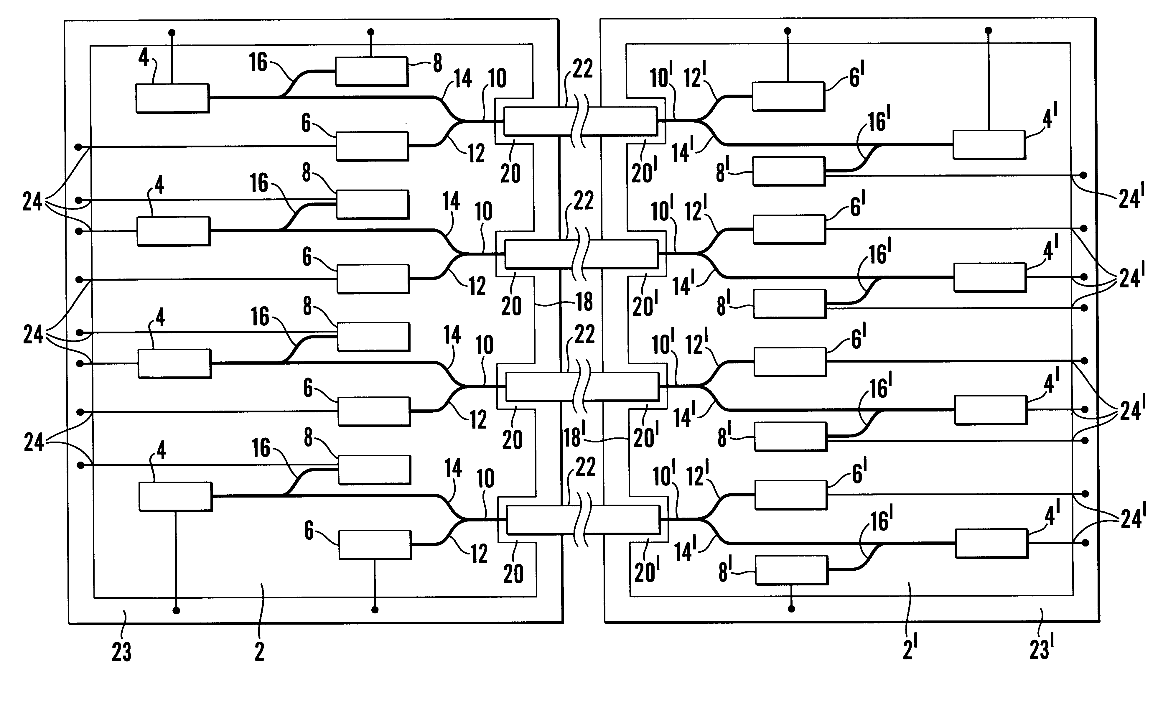
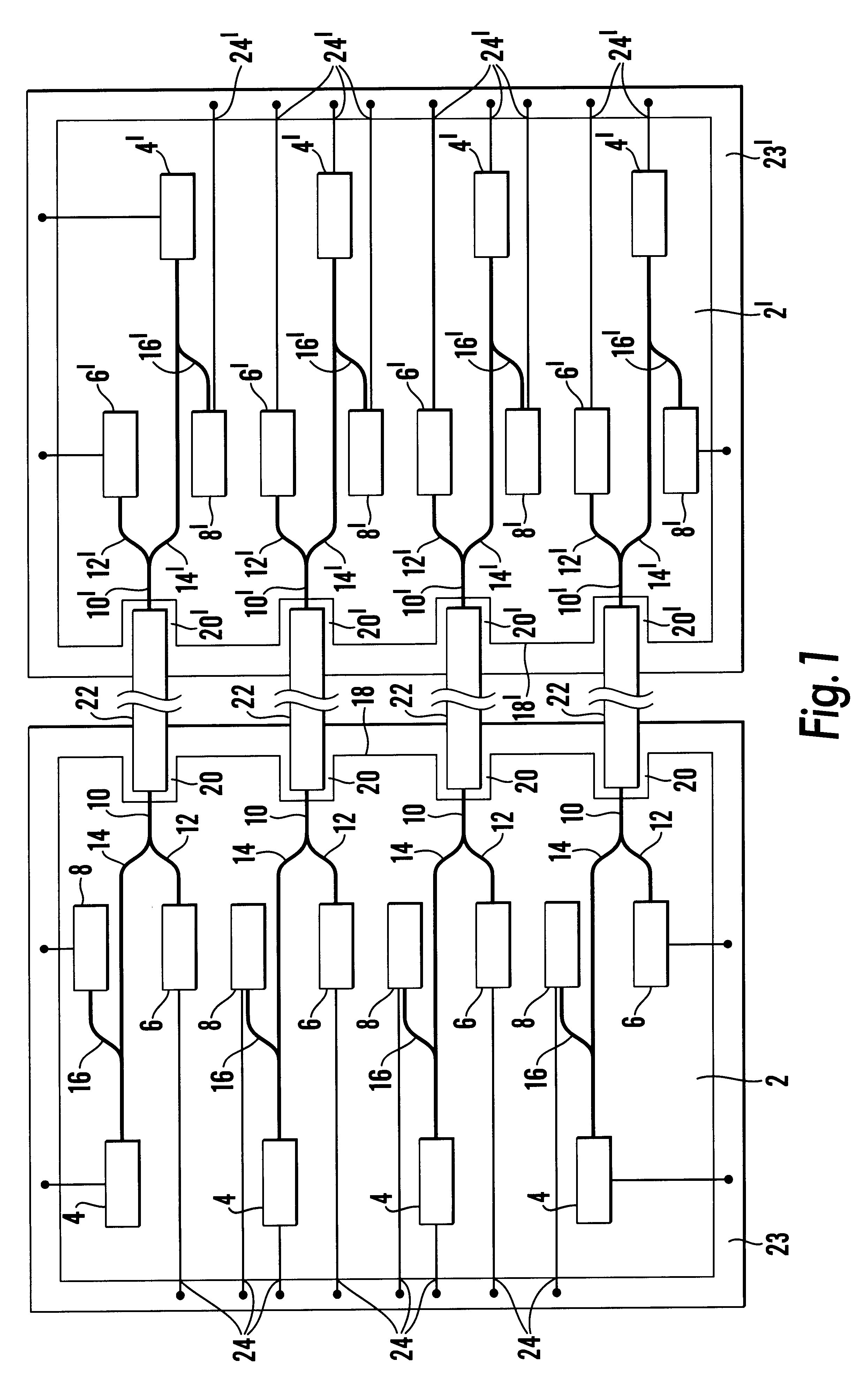
FIG. 2 shows the invention in which uni-directional optical fibre connections are provided between two silicon-on-insulator chips. The components shown in FIG. 2 are given the same reference numerals as the corresponding components shown in FIG. 1. The arrangement is similar to that of FIG. 1 except that the rib waveguides 12 and 14 connect the photodiodes 6 and lasers 4, respectively, to separate optical fibres 22 rather than communicating with a single optical fibre for bi-directional communication between the chip 2, 2'.
third embodiment
FIG. 3 shows the invention in which wavelength division multiplexing (WDM) means 25 are used so the light signals from a plurality of lasers 4, each producing an output of a different wavelength, can be transmitted by a single optical fibre 22 between two chips 2, 2'. The WDM means 25 connects to the fibre 22 by a single rib waveguide 26 if the optical fibre 22 is used to transmit bidirectional signals. The WDM means 25 also acts to de-multiplex the signals received from the fibre 22 and direct them to the appropriate photodiode 6, according to the wavelength of the received signal. The laser 4 and associated photodiode 6 on each chip may operate on the same wavelength and be connected to the WDM means 25 via a Y-junction (similar to the connection of the lasers and photodiodes to the fibres in FIG. 1) or they may operate on different wavelengths (to reduce cross-talk between the photodiodes and the laser). In this case, they may have separate connections to the WDM means 25 as show...
PUM
 Abstract
Description
Claims
Application Information