Silicon anti-fuse structures, bulk and silicon on insulator fabrication methods and application

a technology of silicon and insulator, applied in the direction of semiconductor devices, semiconductor/solid-state device details, electrical devices, etc., can solve the problems of cost and complicated process

Inactive Publication Date: 2002-05-28
IBM CORP
View PDF13 Cites 79 Cited by
  • Summary
  • Abstract
  • Description
  • Claims
  • Application Information

AI Technical Summary

Problems solved by technology

This presents a problem in that the voltage / current required to program the AF must pass through standard CMOS logic without damaging it.
In addition, the voltage must generally be generated on-chip since it cannot be passed through an active electrostatic discharge (ESD) protected pin (which would typically trigger), nor can it pass on a no-connect due to Joint Electron Device Engineering Council (JEDEC) specification limitations.
One solution, as described in U.S. Pat. No. 5,691,217, issued to Micron Technology, Inc., and entitled "Semiconductor Processing Method of Forming a Pair of Field Effect Transistors", is to form a pair of field effect transistors having different thickness gate dielectric layers, which is a costly and complicated process.

Method used


Image

  • Silicon anti-fuse structures, bulk and silicon on insulator fabrication methods and application
  • Silicon anti-fuse structures, bulk and silicon on insulator fabrication methods and application
  • Silicon anti-fuse structures, bulk and silicon on insulator fabrication methods and application

Examples


Embodiment Construction

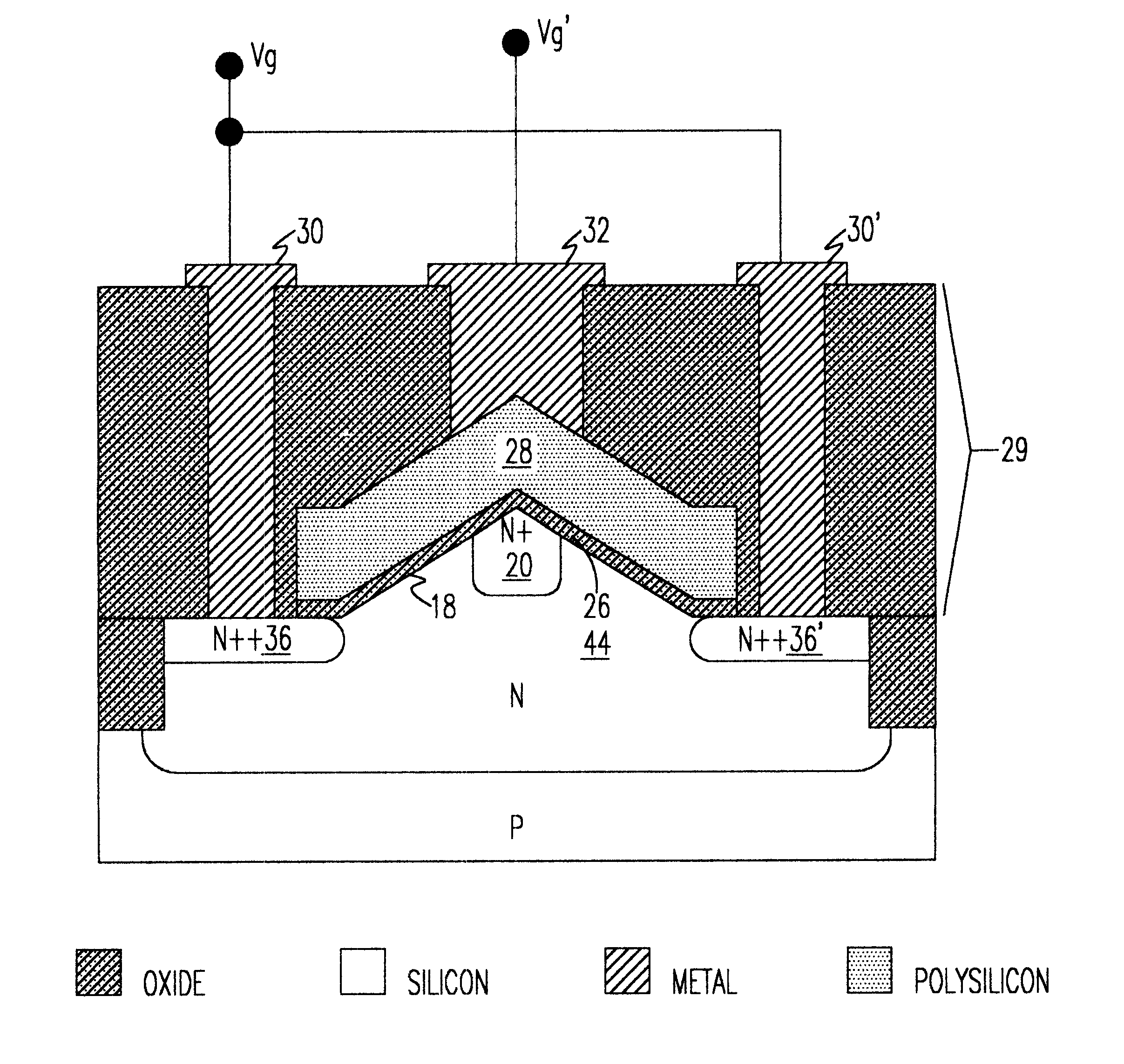
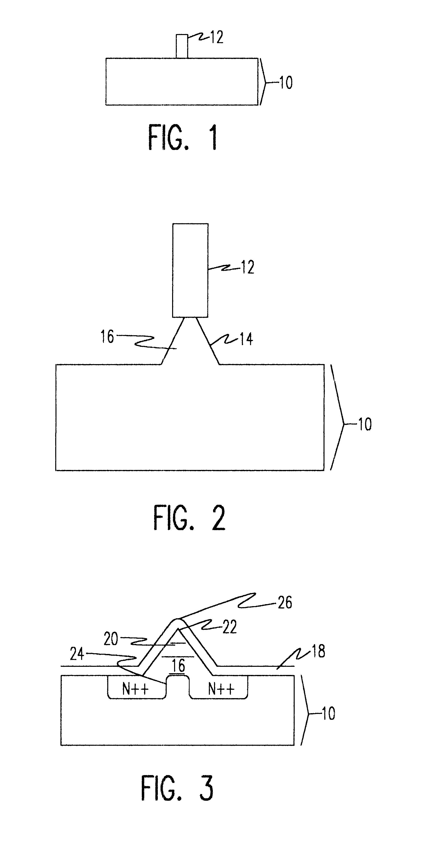
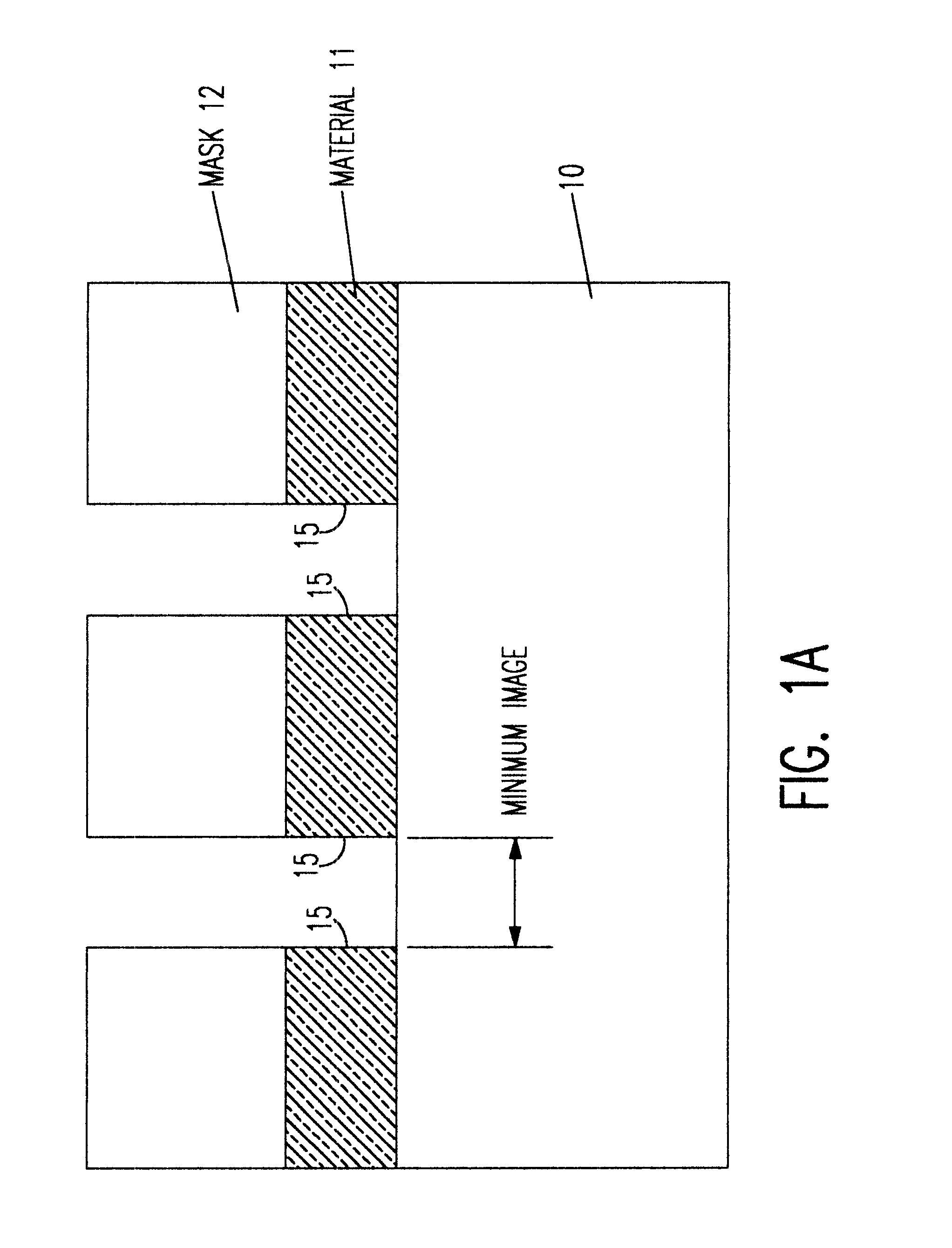
As shown in FIG. 1, a wafer 10 has a mask 12 placed over a portion of the wafer 10. The mask 12 is placed over an area that will eventually form a silicon tip. The mask material may be any suitable material such as, for example, a 20-60 nm nitride. Alternate means of creating a sub-lithographic mask are also feasible, thereby reducing the pitch (i.e., the tip plus space distance) and maximizing tip placement. One such means of producing a sub-lithographic image is shown in FIGS. 1A, 1B and 1C. In FIG. 1A, a mask 12 is used to pattern an oxide material 11, exposing one sidewall 15 for every tip 17 shown in FIG. 1C. In FIG. 1B, a spacer 13, preferably a nitride, is patterned to a sub-lithographic size. Oxide 11 and nitride 13 are chosen such that the etch rate of the oxide 11 is at least 100 times the etch rate of nitride 13. Upon selectively etching the oxide 11, the sub-lithographic mask of the nitride 13 is left, as shown as 17 in FIG. 1C, each of which corresponds to mask 12 show...


PUM


Abstract

A method and semiconductor structure that uses a field enhanced region where the oxide thickness is substantially reduced, thereby allowing antifuse programming at burn-in voltages which do not damage the standard CMOS logic. The semiconductor device comprises a substrate that has a raised protrusion terminating at a substantially sharp point, an insulator layer over the raised protrusion sufficiently thin to be breached by a breakdown voltage applied to the sharp point, a region comprised of a material on the insulator over the raised protrusion for becoming electrically coupled to the substrate after the insulator layer is breached by the breakdown voltage, and a contact for supplying the breakdown voltage to the substrate. In a second embodiment, the semiconductor device comprises a substrate having a trough formed in a top surface of the substrate, a relatively thick insulator layer over the top surface of the substrate, a relatively thin insulator layer over the trough that is breached by a breakdown voltage applied to the trough, a region comprised of a material on the relatively thin insulator layer over the trough for becoming electrically coupled to the substrate after the relatively thin insulator layer is breached by the breakdown voltage, and a contact for supplying the breakdown voltage to said substrate.

Description

1. Field of the InventionThe present invention generally relates to silicon antifuse (AF) structures that will use a field enhanced region having a substantially reduced oxide thickness and, more particularly, to using the reduced oxide thickness to allow AF programming at burn-in voltages which do not damage standard Complementary Metal Oxide Semiconductor (CMOS) logic.2. Background DescriptionAF technology through the use of dielectric breakdown is well understood. U.S. Pat. No. 5,250,459, issued to Lee and entitled "Electrically Programmable Low Resistive Antifuse Element" illustrates this concept. In order to ensure AF programming (i.e., in going from a high impedance state to a low impedance state, a dielectric layer between two conductors is damaged, and a conductive filament between the two conductors is formed), the usual practice to form the filament is to damage a gate oxide layer between the two conductors. This presents a problem in that the voltage / current required to p...

Claims


Application Information

Patent Timeline
Patent Type & Authority Patents(United States)
IPC IPC(8): H01L29/786H01L29/40H01L29/66H01L29/423H01L21/70H01L23/52H01L23/525H01L27/108H01L21/8234H01L27/12
CPCH01L29/78696H01L29/42384H01L21/823412H01L21/823456H01L23/5252H01L27/1203H01L27/10897H01L2924/0002H10B12/50H01L2924/00
Inventor BERTIN, CLAUDE LFURUKAWA, TOSHIHARUHEDBERG, ERIK L.MANDELMAN, JACK A.TONTI, WILLIAM R.WILLIAMS, RICHARD Q.
Owner IBM CORP
Why Eureka
Try Eureka