
Method for suppressing pattern distortion associated with BPSG reflow and integrated circuit chip formed thereby

a technology of bpsg and pattern distortion, which is applied in the direction of thin material processing, semiconductor/solid-state device details, semiconductor devices, etc., can solve the problems of difficult to fabricate damascene structures in bpsg, variations in interconnect resistance, and distortion of the first contact and interconnect levels, etc., to achieve easy alignment and reduce resistance. , the effect of variable resistan

Inactive Publication Date: 2002-12-17
IBM CORP +1
View PDF7 Cites 0 Cited by
  • Summary
  • Abstract
  • Description
  • Claims
  • Application Information

AI Technical Summary

Benefits of technology

It is an advantage of the present invention that mis-alignment problems and variations in resistance are reduced. This reduction is achieved by subjecting the BPSG and undoped oxide to a high temperature before the patterning of the lines, the etching of the contacts and the ion implantation steps. This causes the BPSG and the overlying oxide to densify prior to patterning. Therefore, the shrinkage occurs before the pattern is formed and results in straighter lines which will then be more easily alignable with subsequent layers.
that mis-alignment problems and variations in resistance are reduced. This reduction is achieved by subjecting the BPSG and undoped oxide to a high temperature before the patterning of the lines, the etching of the contacts and the ion implantation steps. This causes the BPSG and the overlying oxide to densify prior to patterning. Therefore, the shrinkage occurs before the pattern is formed and results in straighter lines which will then be more easily alignable with subsequent layers.

Problems solved by technology

A problem with this approach is that distortion of the first contact and interconnect levels can occur during the high temperature junction activation anneal, due to shrinkage of the low temperature oxide and reflow of the BPSG.
This distortion can lead to misalignment with subsequent contact levels (which can cause opens or shorts) and variations in interconnect resistance.
However, it was difficult to fabricate damascene structures in BPSG, due to the high polish rate of BPSG.
Unfortunately, there are a number of problems created by using undoped SiO.sub.2 on BPSG for dual damascene.
One problem is reflow of the BPSG during contact anneals, which can distort studs and interconnects.

Method used


Image

  • Method for suppressing pattern distortion associated with BPSG reflow and integrated circuit chip formed thereby
  • Method for suppressing pattern distortion associated with BPSG reflow and integrated circuit chip formed thereby
  • Method for suppressing pattern distortion associated with BPSG reflow and integrated circuit chip formed thereby

Examples


Embodiment Construction

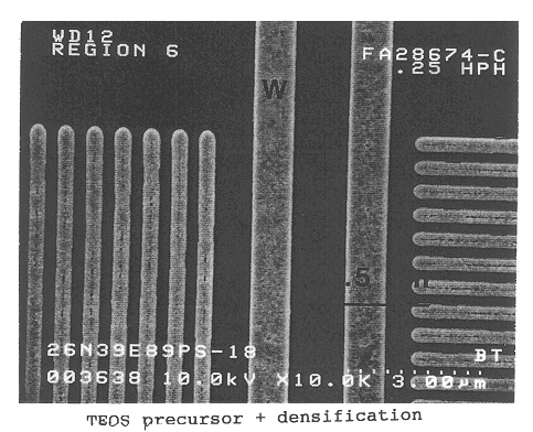
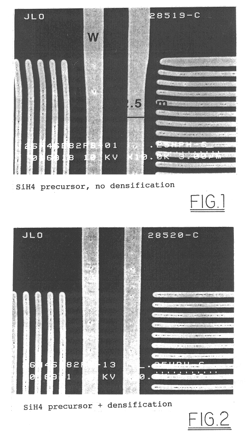
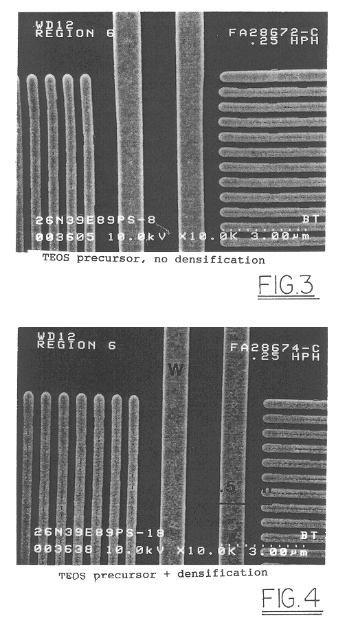
Experiments were conducted on 0.25 .mu.m structures used in developing a 256M DRAM process. After gate patterning and silicon nitride (Si.sub.3 N.sub.4) liner deposition, BPSG was deposited and planarized by CMP. Borderless contacts in the array were etched and filled with doped polysilicon, that was then patterned by CMP to form polysilicon studs. A dual damascene process was used to form bordered contacts to all gates and to the diffusions in the support circuits, as well as tungsten (W) interconnects. The dual damascene process starts with deposition of undoped SiO.sub.2 by plasma enhanced chemical vapor deposition (PECVD). Bordered contacts to all gates and to the diffusions in the support circuits were fabricated using lithography and RIE, with the etch stopping on the gate conductor or Si substrate, respectively. Troughs for interconnects were then patterned using lithography and RIE, with some over-etch into the BPSG to expose the top of the polysilicon studs in the array. Af...


PUM


Abstract

Significant amounts of pattern distortion were found to be the result of reflowing borophosphosilicate glass (BPSG) and silicon dioxide shrinkage during high temperature junction anneals. In order to remedy this problem, a method for suppressing the pattern distortion by subjecting the wafer coated with BPSG and with silicon dioxide layers to a high temperature anneal before patterning is disclosed. The high temperature anneal densifies the undoped silicon dioxide before patterning, so that shrinkage of the undoped silicon dioxide does not affect the patterning steps.

Description

1. Technical FieldThis invention relates generally to the manufacture of integrated circuit (IC) chips and, more specifically, to a method for suppressing pattern distortion associated with the reflow of borophosphosilicate glass (BPSG) dielectric layers during the annealing process of subsequent layers.2. Background ArtIn the present era of very large scale integration and ultra large scale integration, new techniques are continuously being developed to more efficiently utilize the space within semi-conductor devices while maintaining or improving present production efficiency, i.e., reducing the number of IC chips that fail because of various mistakes that may occur during the production process.In the manufacture of IC chips, interconnecting contacts are provided between the active semiconductive material, in which the semiconductor devices are formed, and the interconnect lines. These contacts are typically formed by initially depositing a borophosphosilicate glass (BPSG) dielec...

Claims


Application Information

Patent Timeline
IPC IPC(8): H01L21/02H01L23/532H01L21/70H01L21/768H01L21/316H01L23/52H01L21/28H01L23/522
CPCH01L21/02129H01L21/02164H01L21/022H01L21/02274H01L21/02304H01L21/76801H01L23/5329H01L21/31612Y10T428/24926H01L2924/0002H01L2924/00H01L21/02282
Inventor GAMBINO, JEFFREY PETERNGUYEN, SON VANSTENGL, REINHARD
Owner IBM CORP
Learn More