Method of fabricating a semiconductor device using trench isolation method including hydrogen annealing step

a technology of trench isolation and semiconductor devices, applied in the direction of semiconductor devices, basic electric elements, electrical equipment, etc., can solve the problems of increasing manufacturing costs, reducing the thickness of field oxide films, and unable to electrically isolate adjacent semiconductor devices

Inactive Publication Date: 2003-01-28
SAMSUNG ELECTRONICS CO LTD
View PDF7 Cites 24 Cited by
  • Summary
  • Abstract
  • Description
  • Claims
  • Application Information

AI Technical Summary

Problems solved by technology

In other words, a punch-through phenomenon occurs, or the thickness of a field oxide film is so reduced that adjacent semiconductor devices cannot be electrically isolated.
The above trench isolation method solves the problems of the LOCOS method, but the processes are more complicated than those of the LOCOS method, thereby increasing the manufacturing cost.
Moreover, since the thick mask pattern has been formed on both sides of the trench when the gap filling dielectric layer is formed to fill the trench, a problem that the substantial aspect ratio of the trench increases occurs due to the thick mask pattern.
Consequently, voids may be caused within an isolation layer during the formation of the gap filling dielectric layer.
If the thickness of the pad nitride layer is reduced, however, a problem occurs when the gap filling dielectric layer is planarized by a chemical-mechanical polishing method.
In other words, when the pad nitride layer is thin, physical damage such as scratches may occur on the top of the semiconductor substrate due to abrasives contained in slurry used in a chemical-mechanical polishing method.
If physical damages such as scratches occurs on the top of the semiconductor substrate, a gate oxide can be deteriorated, thereby decreasing the reliability of a semiconductor device.

Method used


Image

  • Method of fabricating a semiconductor device using trench isolation method including hydrogen annealing step
  • Method of fabricating a semiconductor device using trench isolation method including hydrogen annealing step
  • Method of fabricating a semiconductor device using trench isolation method including hydrogen annealing step

Examples


first embodiment

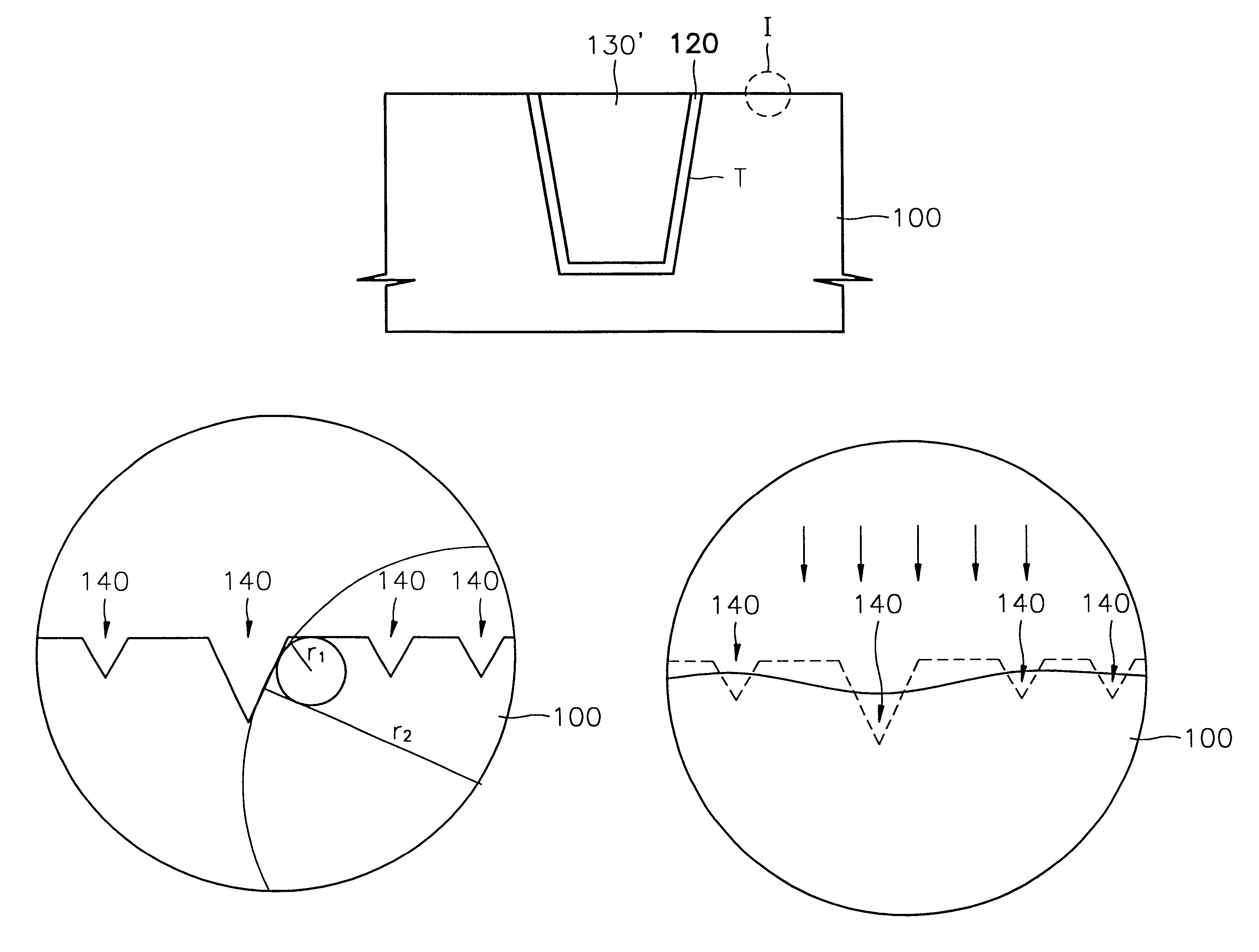
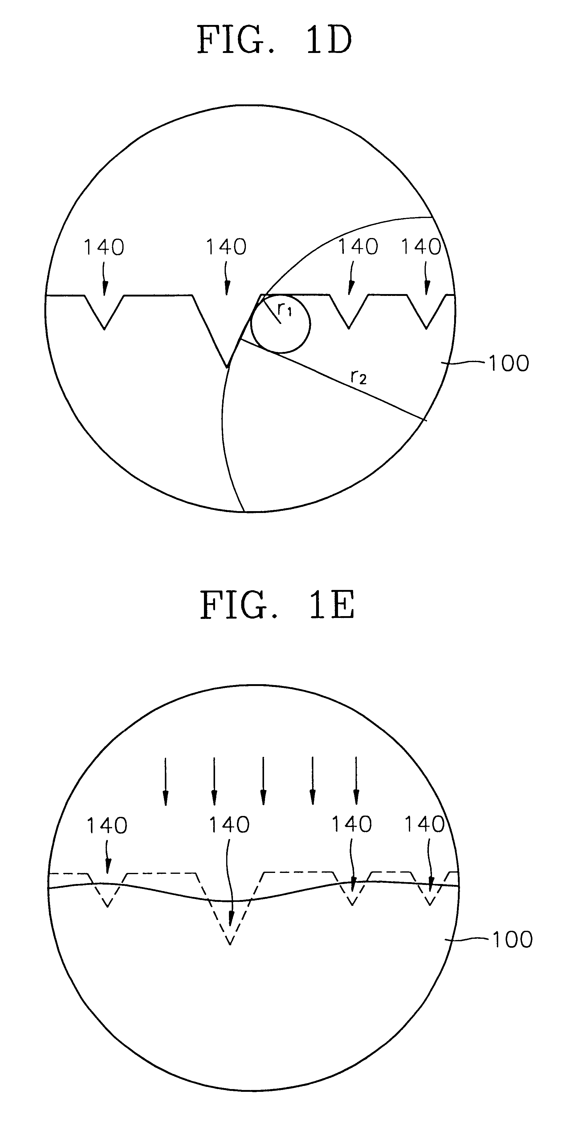
In a test performed by the inventor, it was confirmed that the CMP etching selection ratio of the semiconductor substrate 100 to the gap filling dielectric layer 130 and the CMP etching selection ratio of the semiconductor substrate 100 to the thermal oxide film 120 were about 1:17, when the pH of slurry was maintained at about 7. Accordingly, it was seen that the semiconductor substrate 100 itself can be used as a CMP stopper when slurry of the ceria family is used, so that the amount of CMP can be constantly maintained to obtain an isolation layer 130' having a uniform thickness. It was also confirmed in the test that since the CMP etching selection ratio of the semiconductor substrate 100 to the gap filling dielectric layer 130 is small when CMP slurry of the silica family is used, it is difficult to use the semiconductor substrate 100 as a CMP stopper. In other words, if slurry of the silica family is used when the gap filling dielectric layer 130 is planarized by a CMP method, ...

second embodiment

In the second embodiment of the present invention, a thin nitride liner 125 is formed on the thermal oxide film 120 before forming the gap filling dielectric layer 130 for filling the trench T. The nitride liner 125 is used as a planarization stop layer during planarization of the gap filling dielectric layer 130.

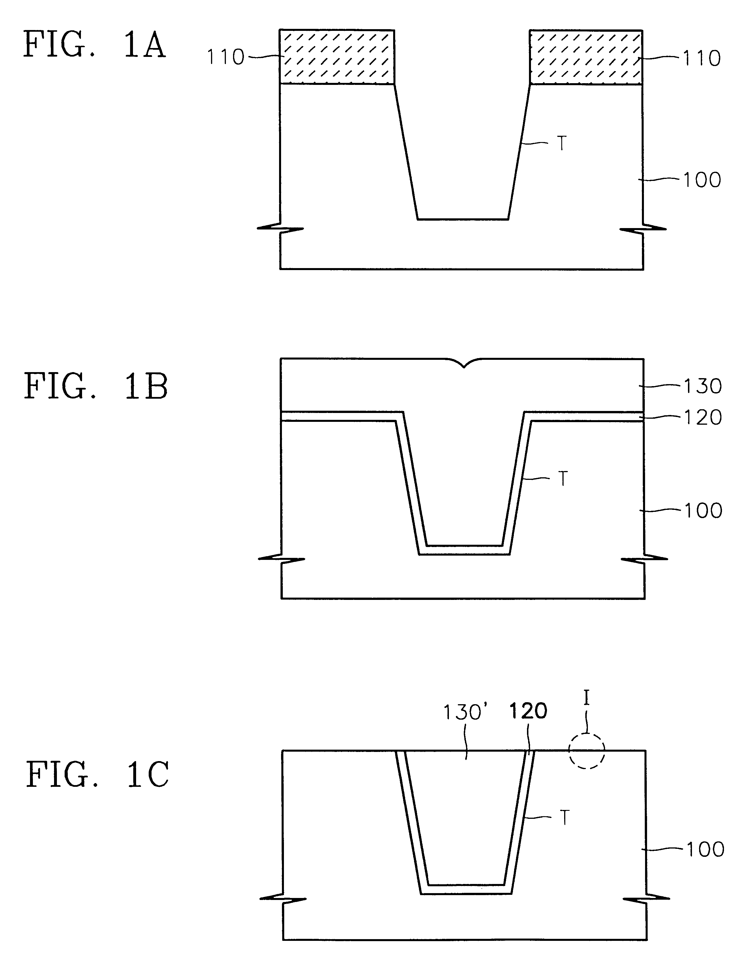
Referring to FIG. 2A, in the same manner as in the first embodiment, a photoresist pattern (not shown) is formed, a trench T is formed in a semiconductor substrate 100 using the photoresist pattern as an etching mask, the photoresist pattern is removed, and, subsequently, a thermal oxide film 120 is formed on the entire surface of the semiconductor substrate 100.

Next, a thin nitride liner 125 is formed along the surface topology of the thermal oxide film 120. The nitride liner 125 may be formed by methods such as CVD, SACVD, LPCVD or PECVD. The nitride liner 125 prevents oxidation of the side wall of the trench T during a succeeding step of filling the trench T with the gap...

third embodiment

Unlike the second embodiment, a pad insulating layer 105 is formed on a semiconductor substrate before forming a photoresist pattern 110 in a third embodiment.

Referring to FIG. 3A, a pad insulating layer 105 is formed on a semiconductor substrate 100. The pad insulating layer 105 may be a silicon oxide layer or a silicon oxy nitride layer. When the pad insulating layer 105 is formed of silicon oxide layer, thermal oxidation may be used. When the pad insulating layer 105 is formed of a silicon oxy nitride layer, a CVD method, an LPCVD method, an SACVD method or a PECVD method may be used. The pad insulating layer 105 is preferably formed to a thickness that does not increase the aspect ratio of a trench T substantially when the trench T is filled with a gap filling dielectric layer later 130. The pad insulating layer 105 may be formed to a thickness of 100-1500 .ANG., and preferably, to a thickness of 500 .ANG.. After forming the pad insulating layer 105, a photoresist pattern 110 is...


PUM


Abstract

A method of fabricating a semiconductor device using a trench isolation method including a hydrogen annealing step, wherein a photoresist pattern is formed on a semiconductor substrate, a pad insulating layer may be formed before forming the photoresist pattern, the semiconductor substrate is etched using the photoresist pattern as an etching mask to form a trench, and an isolation layer is formed in the trench. To remove damages created in an active region defined by the isolation layer, the semiconductor substrate having the isolation layer is annealed in a hydrogen atmosphere.

Description

1. Field of the InventionThe present invention relates to a method of fabricating a semiconductor device, using a trench isolation method.2. Description of the Related ArtLocal oxidation of silicon (LOCOS), which is widely used in fabricating semiconductor devices, has an advantage of simplifying the fabrication. For extremely integrated semiconductor devices such as 256M dynamic random access memory (DRAM) devices, a width for device isolation is reduced to be smaller than a predetermined limit so that a problem can occur during a selective oxidation process in the LOCOS. In other words, a punch-through phenomenon occurs, or the thickness of a field oxide film is so reduced that adjacent semiconductor devices cannot be electrically isolated. Recently, a trench isolation method has been proposed for solving the above problems of the LOCOS.According to one trench isolation method, a pad oxide layer and a pad nitride layer are sequentially deposited on a semiconductor substrate to for...

Claims


Application Information

Patent Timeline
Patent Type & Authority Patents(United States)
IPC IPC(8): H01L21/70H01L21/762H01L21/76
CPCH01L21/76224Y10S438/958H01L21/76
Inventor PARK, TAI-SUPARK, KYUNG-WONPARK, JUNG-WOOSONG, WON-SANG
Owner SAMSUNG ELECTRONICS CO LTD
Why Eureka
Try Eureka