

Using fast hot-carrier aging method for measuring plasma charging damage
a technology of plasma charge damage and hot-carrier aging, which is applied in the direction of measurement devices, semiconductor/solid-state device testing/measurement, instruments, etc., can solve the problems of complex detection and assessment of the degradation of gate dielectrics and their interfaces, and the inability to detect early and assess the accumulation of plasma charge damage in semiconductor devices
- Summary
- Abstract
- Description
- Claims
- Application Information
AI Technical Summary
Problems solved by technology
Method used
Image

Examples
Embodiment Construction
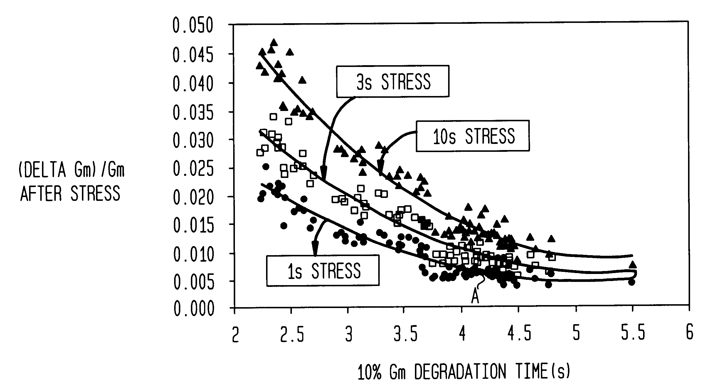
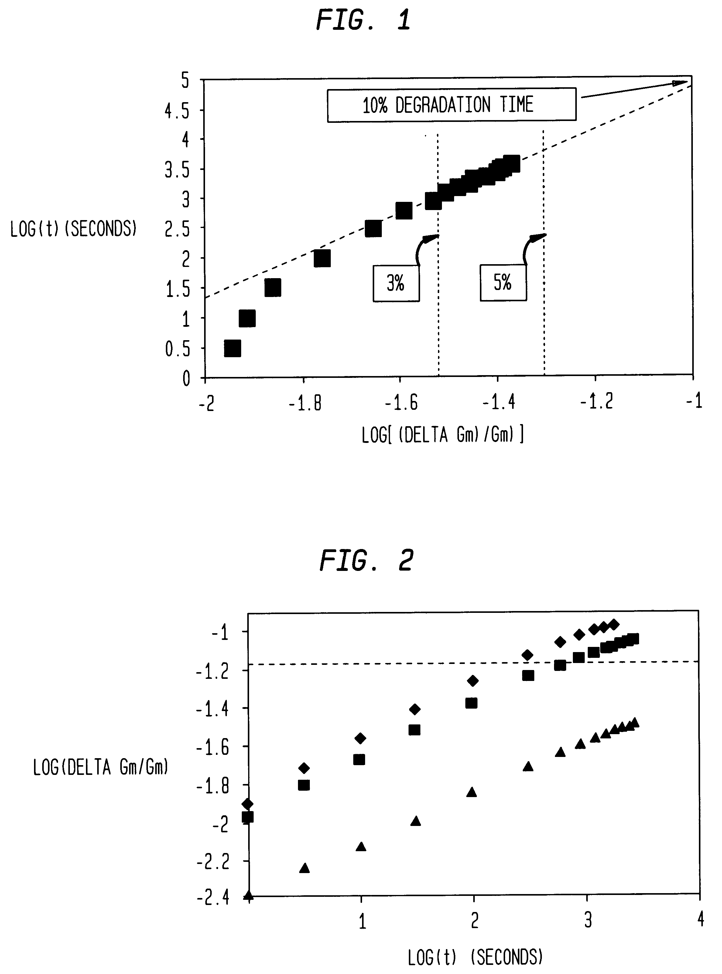
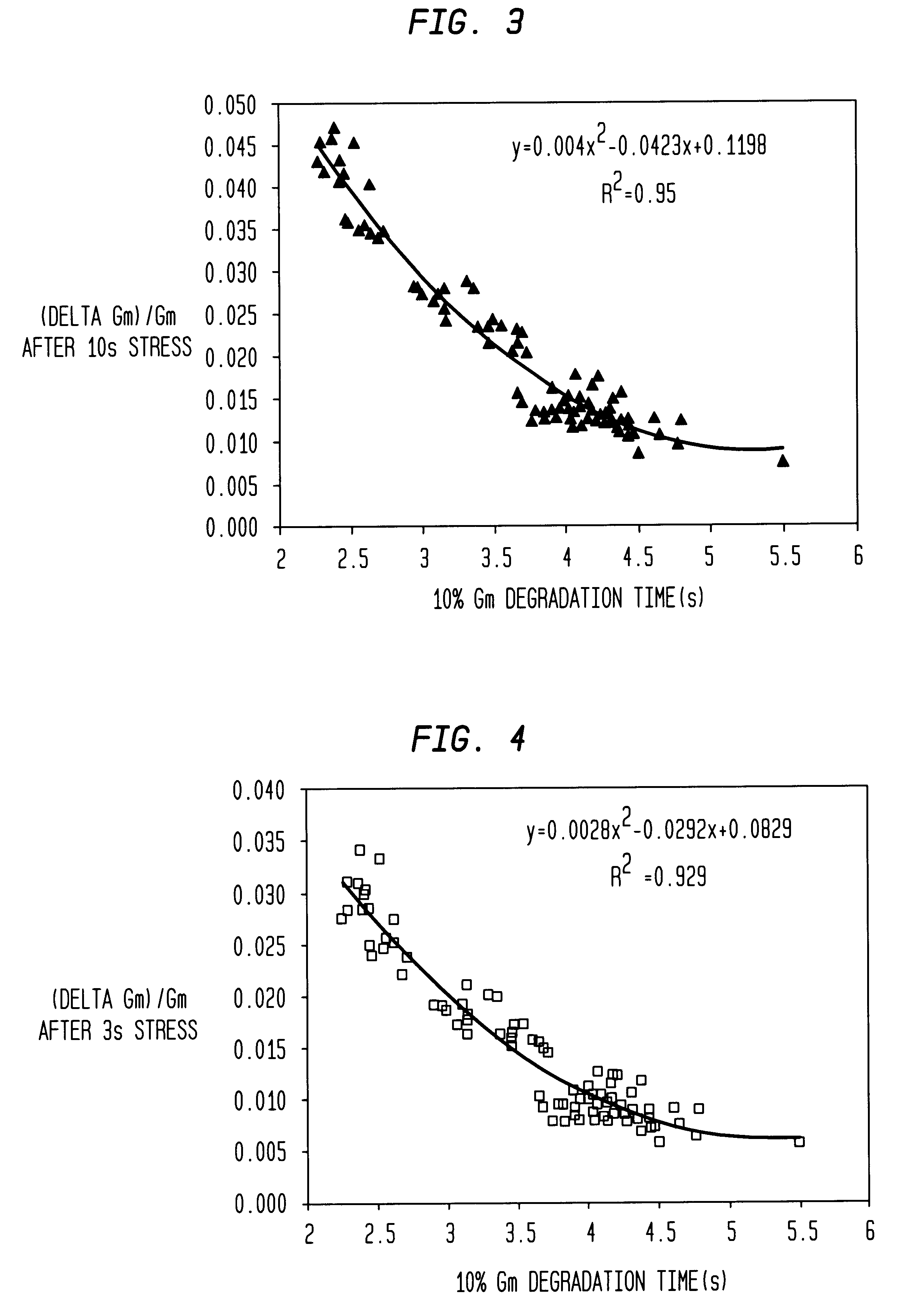
Wafers having a gate-oxide with a 90 .ANG. thickness and including n-channel transistors were processed to post metallization anneal (PMA) at 400.degree. C. for thirty minutes after three levels of metal using 0.35 .mu.m CMOS technology. Some wafers were removed from the processing at metal level 1 for damage testing and some of the wafers were removed at metal level 2 processing for damage testing as well as hot-carrier aging after the post metallization anneal. The initial electron trapping slope (ITES) method was used for damage testing which confirmed that plasma damage due to interlevel dielectric deposition exists.
Hot-carrier stress was performed in peak substrate current condition (V.sub.D =5.6V, V.sub.g =2.3V). Transistor parameters were measured at various points by interrupting the stress. The measurement was performed in a linear regime with the drain bias being set at 200 mV to minimize the impact of drain voltage fluctuation (+ / -1 mV). The source and drain were exchange...
PUM
 Abstract
Description
Claims
Application Information