Mid infrared and near infrared light upconverter using self-assembled quantum dots

a quantum dots and converter technology, applied in the field of electronic devices, can solve the problems of difficult bonding of detectors to si chips, inability to cheaply provide reliable devices, and inability to process hgcdte or insb itself extremely complex and costly,

Inactive Publication Date: 2003-04-01
RGT UNIV OF CALIFORNIA
View PDF13 Cites 70 Cited by
  • Summary
  • Abstract
  • Description
  • Claims
  • Application Information

AI Technical Summary

Problems solved by technology

However, this approach suffers because the difference in material thermal expansion coefficients makes it difficult to bond the detectors to the Si chip.
Further, processing of HgCdTe or InSb is itself extremely complex and costly.
However, QWIPs have also fallen short of cheaply providing a reliable device because QWIPs are insensitive to normal incident light.
Further, large lateral diffusion of photoexcited carriers in the QW deteriorate the spatial resolution of the QWIP imaging device.
However the difference in material thermal expansion coefficients makes it difficult to bond the detector to the Si chip.
In addition, the processing of HgCdTe or InSb is itself complex and costly.
However, QWIPs have difficulty with normal incident light.

Method used


Image

  • Mid infrared and near infrared light upconverter using self-assembled quantum dots
  • Mid infrared and near infrared light upconverter using self-assembled quantum dots
  • Mid infrared and near infrared light upconverter using self-assembled quantum dots

Examples


Embodiment Construction

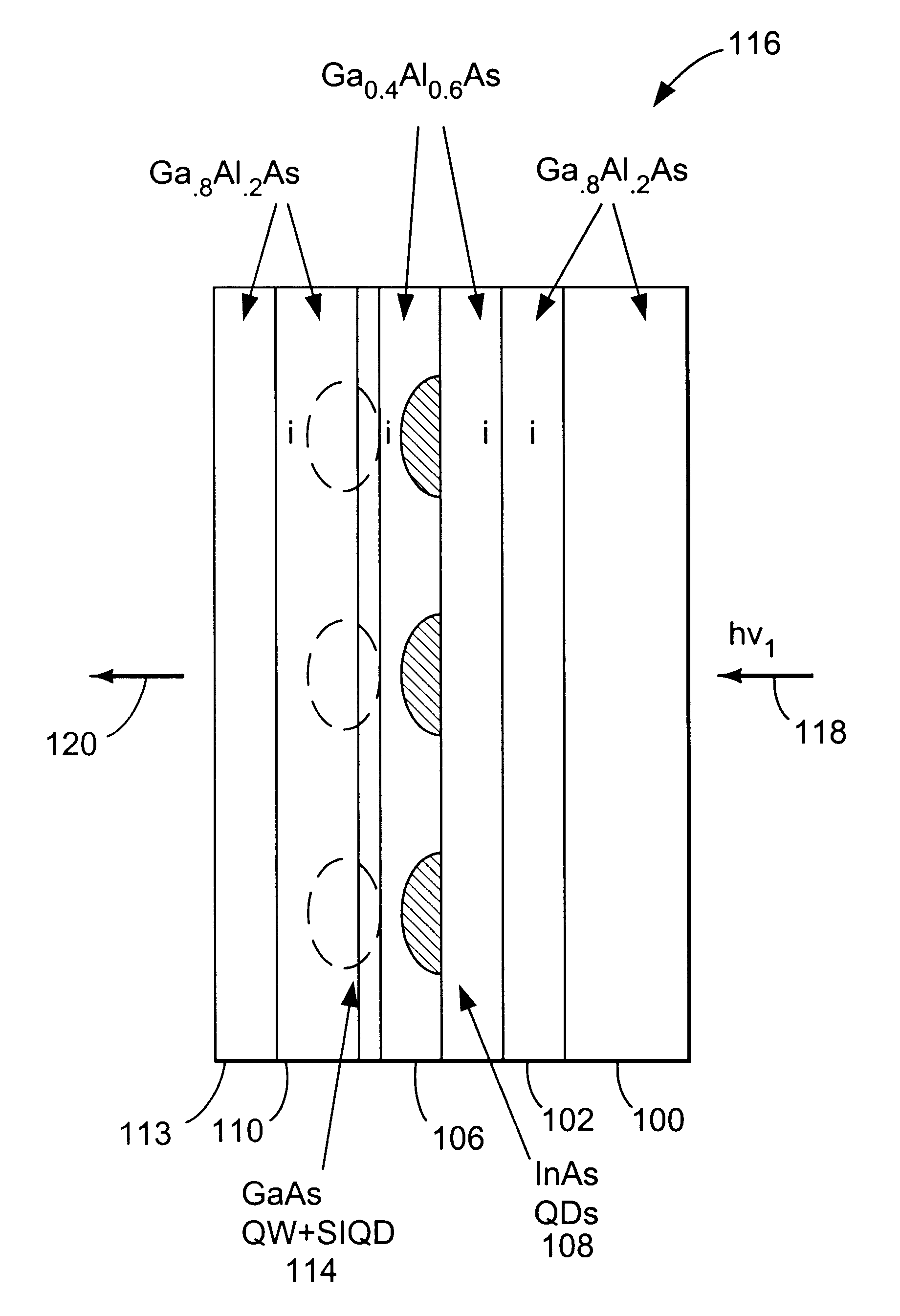
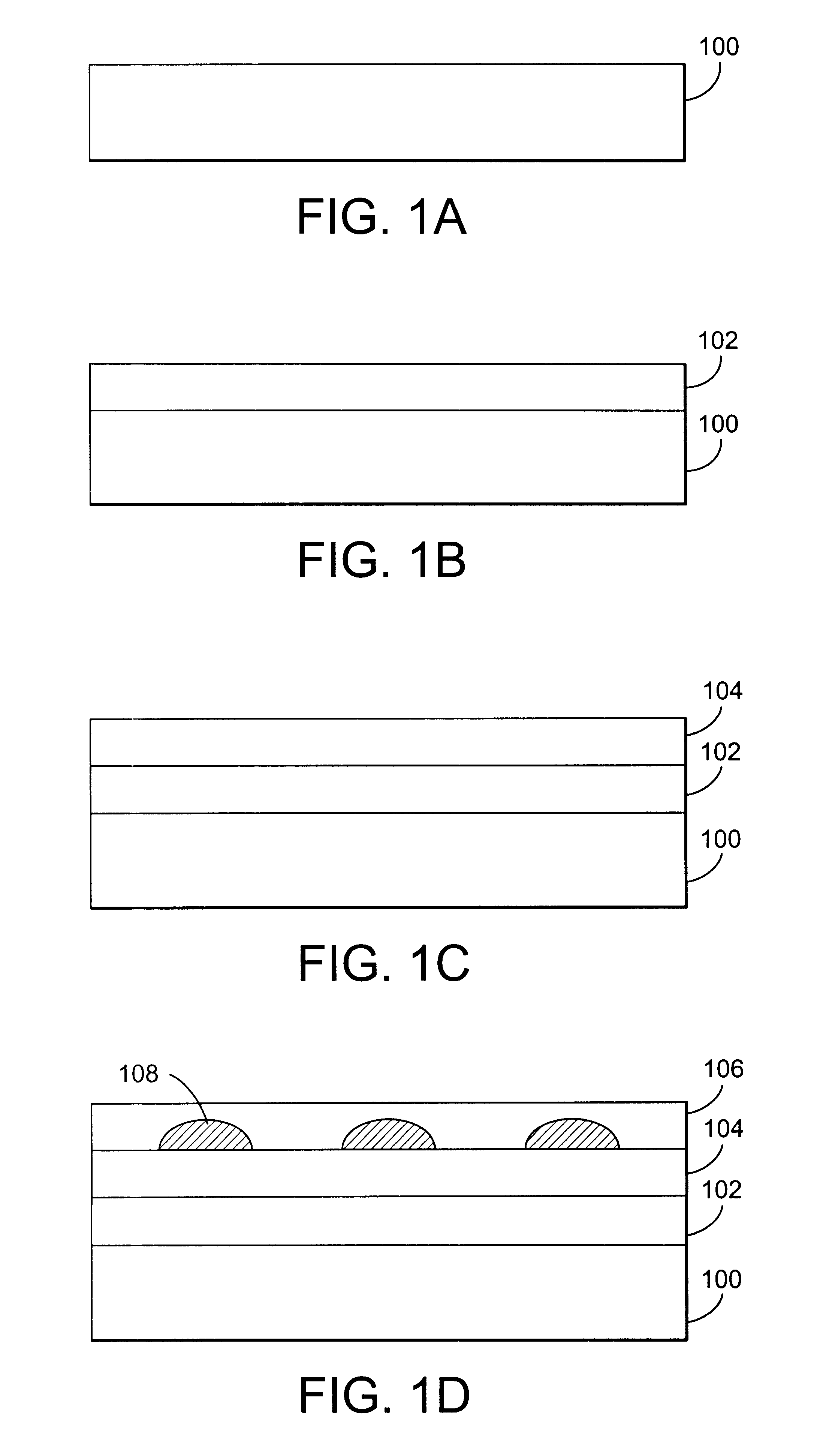
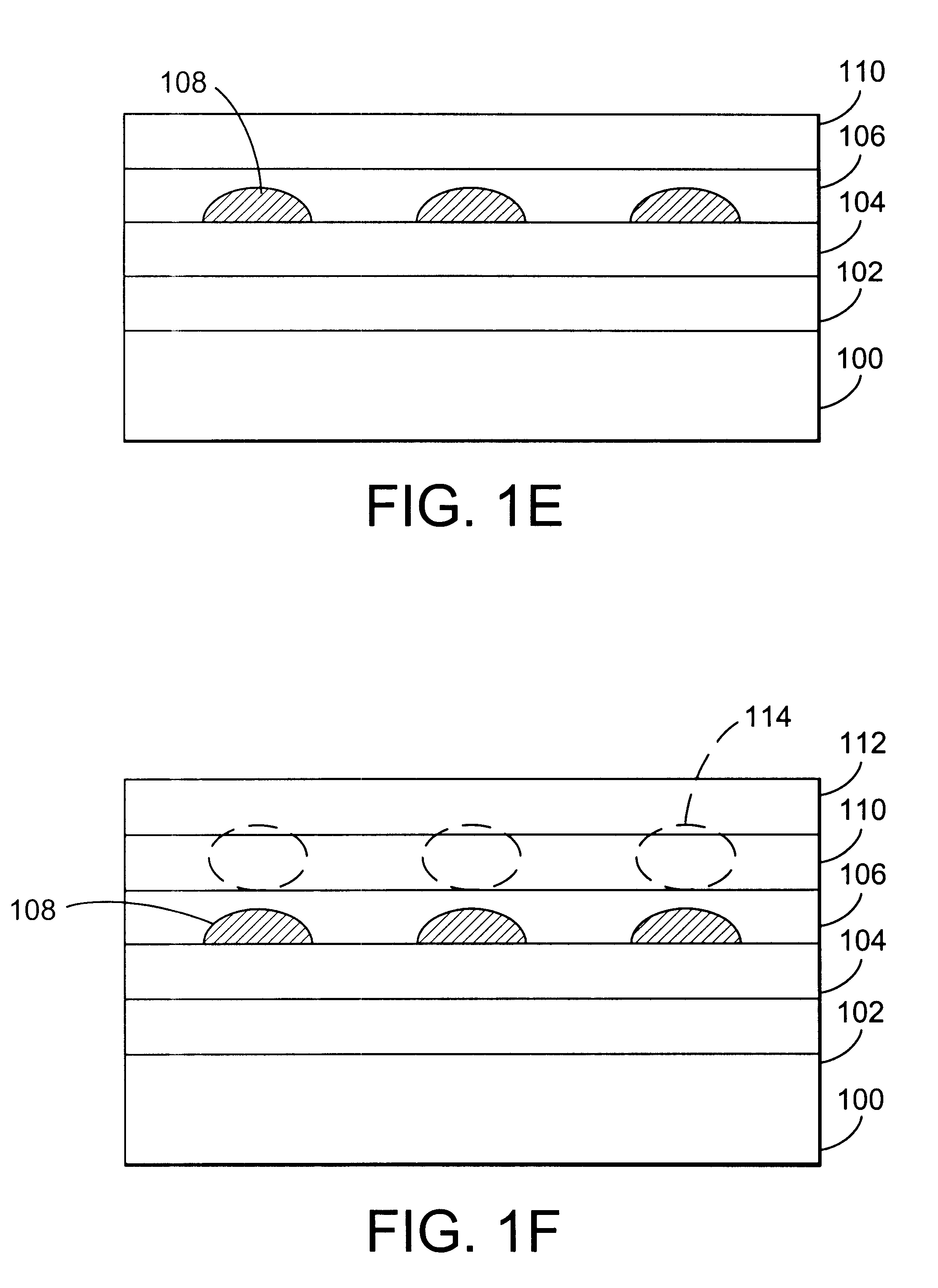
Although described with respect to GaAs / InAs materials systems, the present invention can be used with any materials system, including but not limited to any material system where quantum dots can be fabricated using MBE, MOCVD or MOMBE techniques, such as InP / GaInP, InGaAlAs / AlGaAs, InGaN / GaN, SiGe / Si, or other combinations of materials. The strain induced quantum dots 114 can be induced in any of the materials listed. The SiGe / Si system can be directly integrated to silicon CCD camera elements for ease of manufacture. Multiple conversions from one wavelength to another using multiple quantum dot / stress induced quantum dot excitations are also possible using the present invention. For example, a GaAs / InP system can be used to convert M&FIR wavelengths to near visible or visible wavelengths.

The stress induced quantum dot layer 110 can be replaced by a layer of coupled quantum dots which are coupled and close to the quantum dots 108. These coupled quantum dots have appropriate dimens...


PUM

PropertyMeasurementUnit
distanceaaaaaaaaaa
wavelengthaaaaaaaaaa

Abstract

A method and device for converting light from a first wavelength to a second wavelength. The method comprises the steps of exciting an electron in a quantum dot with an incident infrared photon having the first wavelength, the excited electron having a first energy, tunneling the excited electron through a barrier into a stress induced quantum dot, and recombining the excited electron with a hole in the stress induced quantum dot, therein producing a photon having the second wavelength, typically in the visible range. The device comprises a substrate, a spacer layer, coupled to the substrate, a second layer, coupled to the spacer layer, wherein the second layer comprises a different material than the spacer layer, a third layer, coupled to the second layer, wherein the third layer comprises at least one quantum dot, a fourth layer, coupled to the third layer, comprising a quantum well corresponding to each quantum dot in the third layer, a fifth layer, coupled to the fourth layer, wherein the fourth layer and fifth layer comprise a strain induced quantum dot corresponding to each quantum dot in the third layer; and a sixth layer, coupled to the fifth layer, the substrate and the sixth layer for contacting the device.

Description

1. Field of the Invention.This invention relates generally to electronic devices, and more particularly to a mid and far infrared to near infrared light converter using InAs self-assembled quantum dots.2. Description of Related Art.Advances in the field of electronics have brought new means for the detection and use of infrared radiation in the mid-and far-infrared regions. The use of semiconductor materials has made the detection of infrared radiation more efficient and cost efficient. Even more compact and efficient means of detection and imaging in the infrared region of the spectrum can be devised using new semiconductor structures.Large two-dimensional focal plane arrays in the mid- and far-infrared (M&FIR) region have important applications in the fields of pollution detection, thermal imaging, and imaging of astronomical objects. A typical approach for detecting M&FIR radiation uses indium antimonide (InSb) or mercury cadmium telluride (HgCdTe) detector arrays bonded to a sil...

Claims


Application Information

Patent Timeline
Patent Type & Authority Patents(United States)
IPC IPC(8): G02F2/00G02F2/02H01L31/0352H01L31/0248
CPCB82Y10/00H01L31/0352G02F2/02B82Y20/00
Inventor PETROFF, PIERRE M.HORIGUCHI, NAOTO
Owner RGT UNIV OF CALIFORNIA
Why Eureka
Try Eureka