Advanced contact integration scheme for deep-sub-150 nm devices

a technology of advanced contact and sub-150 nm, which is applied in the direction of semiconductor/solid-state device manufacturing, basic electric elements, electric devices, etc., can solve the problems of shallow junctions, no universal proposal to make advanced contact meeting ultimate requirements, and existing process integration schemes that fail to meet contact requirements

Inactive Publication Date: 2003-04-08
PROMOS TECH INC
View PDF24 Cites 18 Cited by
  • Summary
  • Abstract
  • Description
  • Claims
  • Application Information

AI Technical Summary

Problems solved by technology

As device design density shrinks for CMOS devices covering both deep trench dynamic random access memory (DT DRAM) and addressing logic, existing process integration schemes fail to meet contact requirements, especially as CMOS devices are scaled down to 150 nm node.
However, there is presently no universal proposal to make an advanced contact meeting ultimate requirements due to complex interrelationships among these parameters, each having its own process integration steps.
This integration scheme results in shallow junctions with low contact resistance for deep-sub-150 nm devices.

Method used


Image

  • Advanced contact integration scheme for deep-sub-150 nm devices
  • Advanced contact integration scheme for deep-sub-150 nm devices
  • Advanced contact integration scheme for deep-sub-150 nm devices

Examples


Embodiment Construction

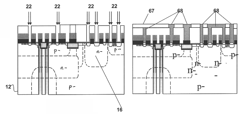
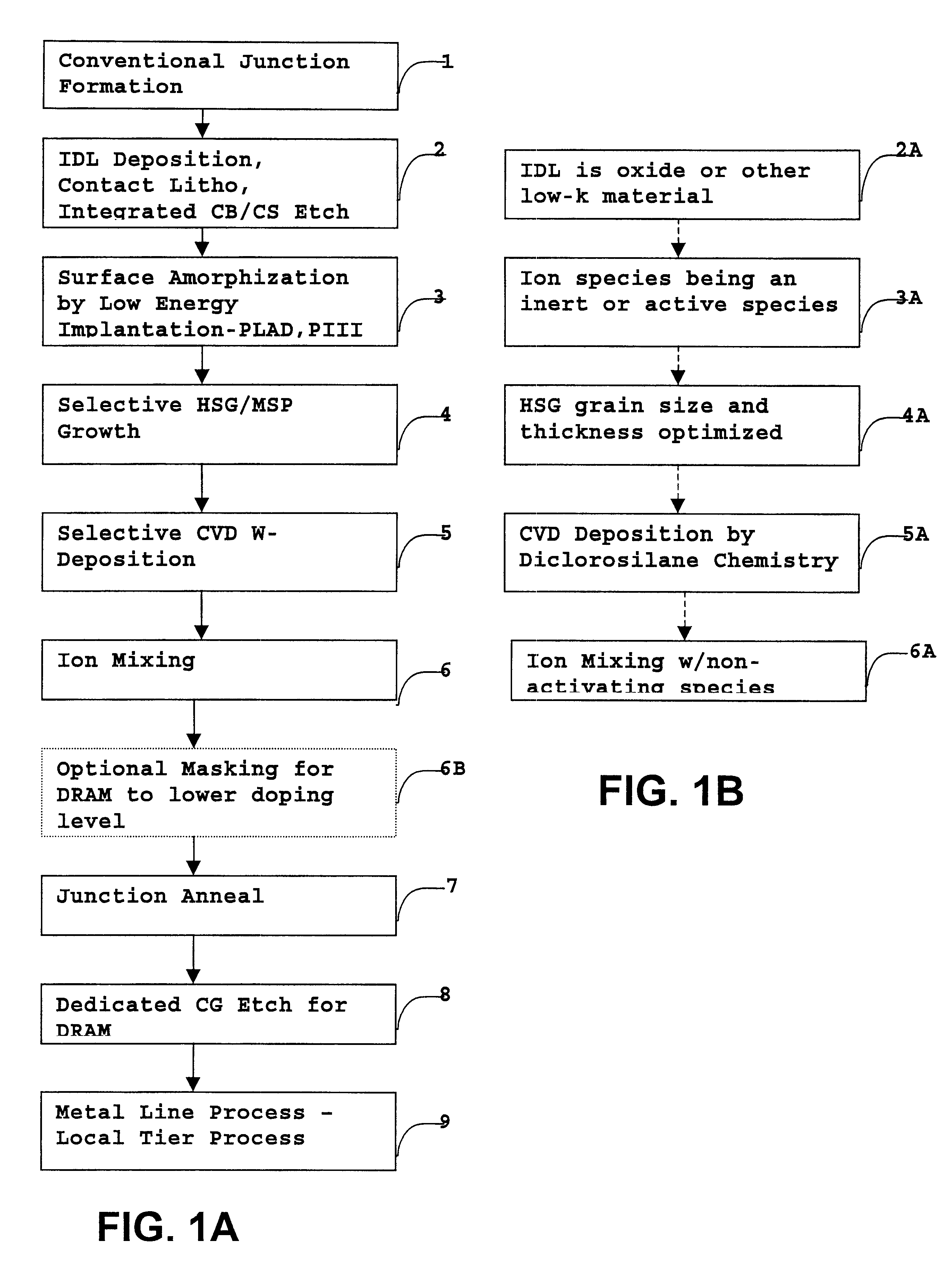
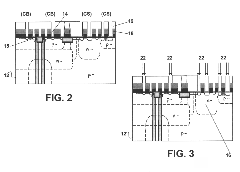
Advanced metal silicon (MS) contacts require high doping to form low resistance ohmic contacts. At these heavily doped MS junctions, the electron emission (TE) is dominated by field emission (FE) and thermal-field emission (TFE), leading to higher contact conductivity. However, a very high surface concentration of dopants naturally leads to deeper junctions because of concentration dependent diffusion. This effect transiently increases following a high-energy implantation step due to the anomalous diffusion effect of transient enhanced diffusion (TED). This transient effect results from the thermal treatment (anneal) of the silicon that is necessary to activate the implanted ions (i.e., to move the dopant atoms to substitutional sites), and to remove residual implantation damage. In this way, the objective of low R.sub.C and shallow (X.sub.JC) work against one another.

Furthermore, silicidation on heavily doped Si is often considerably more difficult than that of undoped Si.

To overco...


PUM


Abstract

An advanced contact integration technique for deep-sub-150 nm semiconductor devices such as W / WN gate electrodes, dual work function gates, dual gate MOSFETs and SOI devices. This technique integrates self-aligned raised source / drain contact processes with a process employing a W-Salicide combined with ion mixing implantation. The contact integration technique realizes junctions having low contact resistance (RC), with ultra-shallow contact junction depth (XJC) and high doping concentration in the silicide contact interface (Nc).

Description

1. Field of the InventionThe present invention relates to the fabrication of semiconductor devices with self-aligned, raised source / drain.2. Discussion of Related ArtThe self-aligned contact (SAC) is widely known as a fabrication technique for reducing the cell size of memory units. Memory devices fabricated using SACs are commonly formed on the same CMOS chip as the logic circuits that address them.Higher logic circuit performance is often obtained by using salicide (self-aligned silicide) processes. Anneal of a refractory metal layer causes the underlying silicon to react with the metal layer and produces a silicide overlying gate electrode and source and drain regions. These silicided regions have lower resistance than non-silicided regions. This is especially true of smaller geometries.Silicidation is widely used in the art. As device design density shrinks for CMOS devices covering both deep trench dynamic random access memory (DT DRAM) and addressing logic, existing process in...

Claims


Application Information

Patent Timeline
Patent Type & Authority Patents(United States)
IPC IPC(8): H01L21/285H01L21/768H01L21/02H01L21/70H01L21/8238
CPCH01L21/28518H01L21/823871H01L21/76895
Inventor LEE, BRIAN S.
Owner PROMOS TECH INC
Why Eureka
Try Eureka