High speed sink/source register to reduce level sensitive scan design test time

a source register and sink technology, applied in the field of combinatorial logic array testing, can solve the problems of inconvenient lssd test structure, inconvenient creation of test programs, and inconvenient use of test programs

Inactive Publication Date: 2003-07-08
IBM CORP
View PDF8 Cites 24 Cited by
  • Summary
  • Abstract
  • Description
  • Claims
  • Application Information

AI Technical Summary

Benefits of technology

It is another object of the invention to provide a technique and apparatus for reducing time and tester apparatus overhead for level sensitive scan design testing of integrated circuits.
It is yet another object of the invention to provide for reduction of LSSD testing time without optimization or redesign for shift rate increase of test registers or scan chains.

Problems solved by technology

However, with the increased functionality of integrated circuit device and the corresponding increase in number of inputs and dependencies on numerous prior execution cycles, it is unacceptably time-consuming and complex to create test programs to pre-condition inputs to the correct state for testing even only one combination of inputs.
The corresponding test time is also prohibitive.
However, to reduce the LSSD test structure, design costs and possibly chip area occupied by the test path and associated controlling logic (which are not used during normal operation of the chip), input and ouput circuits of portions of the test path are not generally optimized to operate at the high normal speed cycle time of the chip.
Therefore, substantial time was required for loading and unloading the test register.
However, the number of input and output pins provided on test apparatus is limited and cost of test apparatus increases dramatically with the number of input and output pins provided since the tester apparatus must be substantially replicated for each input / output pair of pins.
The number of parallel sections of the test register that can be provided is thus limited, as a practical matter, to the number of input or output pins provided in the tester apparatus.
Therefore there is a trade-off between the number of parallel sections of the test register on the chip (which can be loaded and unloaded at a lower rate or longer cycle time) and the cost of the test apparatus.
Since the cost of tester overhead during a test is the primary reason for seeking to reduce level sensitive scan test time, there is little gain to be obtained by reduction of loading and unloading time by using plural parallel test register sections which can only be accommodated by a more expensive tester apparatus.
Similarly, if the loading and unloading time is halved by reducing the number of signals to be provided to a reduced number or size of logic array partitions simultaneously tested but the number of tests per chip were correspondingly doubled, there would be no reduction (and probably an increase) in the cost of tester apparatus overhead.
Accordingly, reduction of the length of test register sections for a given number of signals to be applied to and collected from logic array partitions is limited by the capacity of the tester apparatus (and, in turn, limits the number of logic array partitions which can be simultaneously tested) and the loading and unloading time of the test register dominates the cost of level sensitive scan testing.
While it is possible to reconfigure a test register, provision of such a facility would require additional expenditure of design time in regard to the test register which is non-functional during normal operations.
By the same token, optimization of the test register input / output circuits to increase signal propagation speed therethrough increases chip cost without producing any functional benefit during normal operation of the chip.
In general, given the capacity of test registers required to significantly reduce testing time, the cost of increasing signal propagation speed thereof (including additional design time and resources to optimize the LSSD test structure for speed and the possible increase of chip area to do so) cannot be fully compensated by reduction of cost of tester apparatus overhead.
Therefore, at the present state of the art, no technique or apparatus is available that can significantly reduce the time and / or cost of level sensitive scan testing of integrated circuit chips.

Method used


Image

  • High speed sink/source register to reduce level sensitive scan design test time
  • High speed sink/source register to reduce level sensitive scan design test time
  • High speed sink/source register to reduce level sensitive scan design test time

Examples


Embodiment Construction

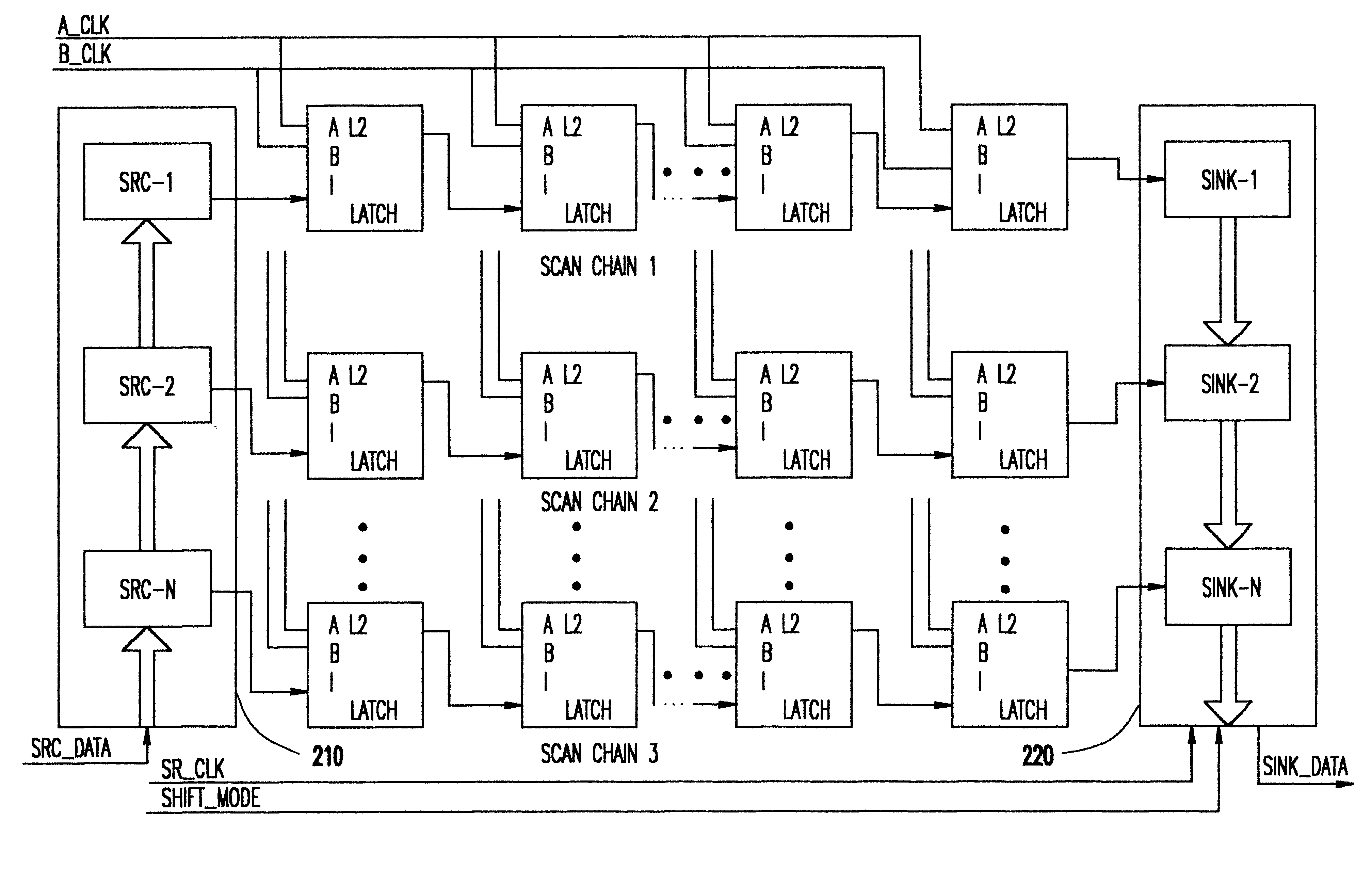
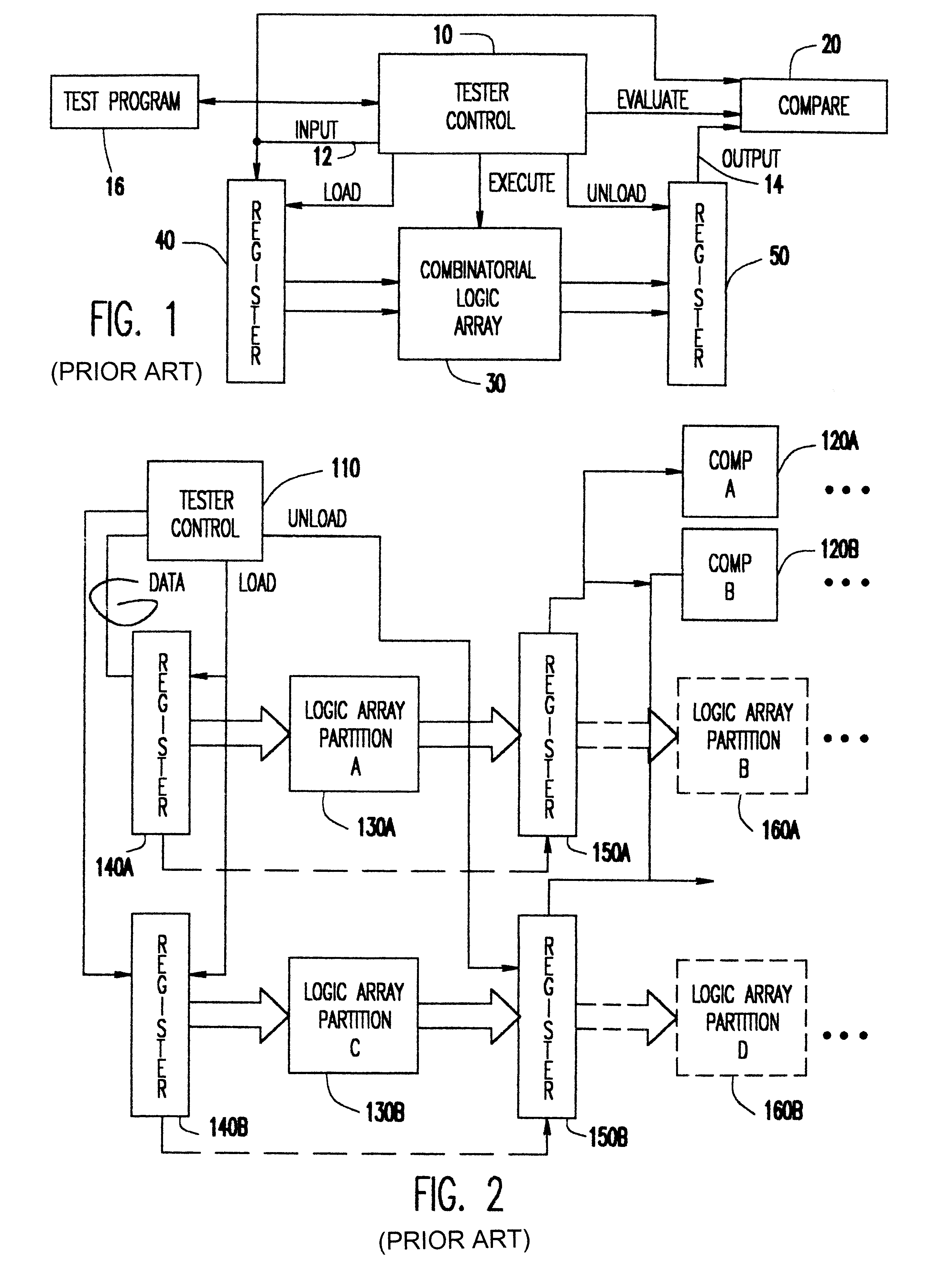
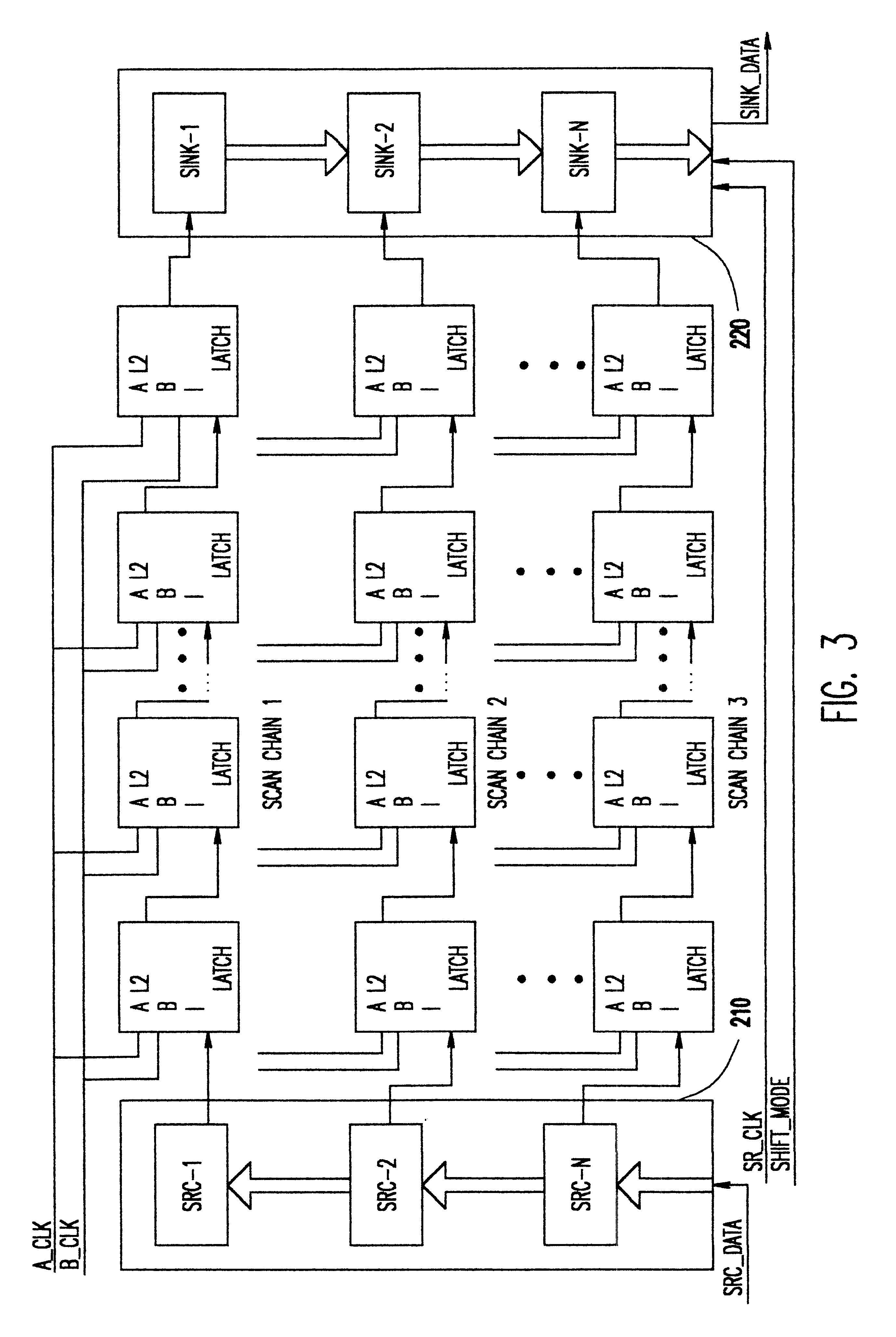
Referring now to the drawings, and more particularly to FIGS. 1 and 2, there are shown schematic block diagrams representing first and second conventional technique of level sensitive Scan Design (LSSD) testing. It should be recognized that the depictions of FIGS. 1 and 2 are arranged to contrast the present invention, as depicted in FIG. 3, therewith in order to more fully convey an understanding of the invention. Therefore, no portion of any Figure is admitted to be prior art as to the present invention.

In the arrangement of FIG. 1, tester control 10 and comparator 20 are considered to be respective elements of any tester apparatus suitable to perform LSSD testing. Connections 12 and 14 represent a single pair of pins including an input pin and an output pin for connection to the chip and providing and retrieving LSSD data patterns in accordance with a test program 16. Comparator 20 provides the function of identifying the portion of the test data sequence which has been employed ...


PUM


Abstract

Test data is provided through shift registers, operated at a high clock rate comparable to or exceeding a normal high speed clock rate of a chip being tested, to each of a plurality of scan chains configured from registers present on the chip; respective latches of which are connected to inputs and outputs of logic array partitions to be tested. Reduced test clock rate of input and output circuits of the scan chains is accommodated by high speed source and sink shift registers. The source and sink registers are fully loaded and unloaded between consecutive test clock signals and test signals are preferably applied to and collected from the chip in a single serial string through a single pair of tester input / output pins. Testing time is thus reduced without requiring design time and chip space for a clock tree optimized for high speed operation while use of testers of reduced cost and having an arbitrarily small number of input / output pin pairs and independent of test register configuaration on the chip can be used.

Description

1. Field of the InventionThe present invention generally relates to testing of semiconductor integrated circuits during manufacture and, more particularly, to the testing of combinatorial logic arrays using level sensitive scan testing techniques.2. Description of the Prior ArtIncreased integration density has greatly increased the functionality, performance and economy of manufacture of integrated circuit devices due to the increased number of active elements which may be placed in greater proximity on chips simultaneously formed on a wafer. However, freedom from manufacturing defects must be ascertained by propagating a sufficient number of different combinations of logic level signals therethrough to be able to determine that the device will perform correctly for any digital signals applied thereto.For relatively simple circuits that involve relatively few inputs and relatively few dependencies on prior execution cycles, a relatively small and simple test program may be construct...

Claims


Application Information

Patent Timeline
Patent Type & Authority Patents(United States)
IPC IPC(8): G01R31/28G01R31/3185
CPCG01R31/318536G01R31/318544
Inventor VONREYN, TIMOTHY J.
Owner IBM CORP
Why Eureka
Try Eureka