A-WO3-gate ISFET devices and method of making the same

a technology of ion-sensitive field effect transistor and wo.sub.3 layer, which is applied in the direction of solid-state devices, instruments, material analysis, etc., can solve the problems of poor sensitivity and stability of devices, and difficult control of wo.sub.3 layer composition made by vacuum evaporation, etc., to achieve low output resistance, high input resistance, and easy production

Inactive Publication Date: 2003-09-09
NATIONAL YUNLIN UNIVERSITY OF SCIENCE AND TECHNOLOGY
View PDF16 Cites 18 Cited by
  • Summary
  • Abstract
  • Description
  • Claims
  • Application Information

AI Technical Summary

Benefits of technology

FIG. 4 is the schematic cross-sectional view of the measuring system used to measure the capacitance and voltage of the device. The measurement is controlled by a computer 46 and analyzed by an inductance-capacitance-resistance analyzer 45 (HP 4284A). During measuring, the device 42 and reference electrode 43 are simultaneously put into a beaker 41 filled with aqueous solution 44. The detection is performed in a dark box 40 to reduce the effect caused by light.
1. The a-WO.sub.3 / SiO.sub.2 -gate ISFET according to this invention is formed by replacing the traditional metal layer existing in the gate of FET with a RF-sputtering a-WO.sub.3 membrane. In addition to being easy to produce, other advantages include high input resistance, low output resistance, short reaction time, trace detectable, and MOS processes compatibility.

Problems solved by technology

When single gate detecting membrane consists of silicon dioxide, the sensitivity and stability of the device are poor.
In general, the composition of the WO.sub.3 layer is hard to control regardless of which method is used in its formation.
For example, the composition of the WO.sub.3 layer made by vacuum evaporation is hard to control and the surface of the WO.sub.3 layer is not uniform.
Moreover, the gate of the conventional ISFET consists of a single SiO.sub.2 layer; thereby the sensitivity and linearity cannot meet the practical requirements.

Method used


Image

  • A-WO3-gate ISFET devices and method of making the same
  • A-WO3-gate ISFET devices and method of making the same
  • A-WO3-gate ISFET devices and method of making the same

Examples


Embodiment Construction

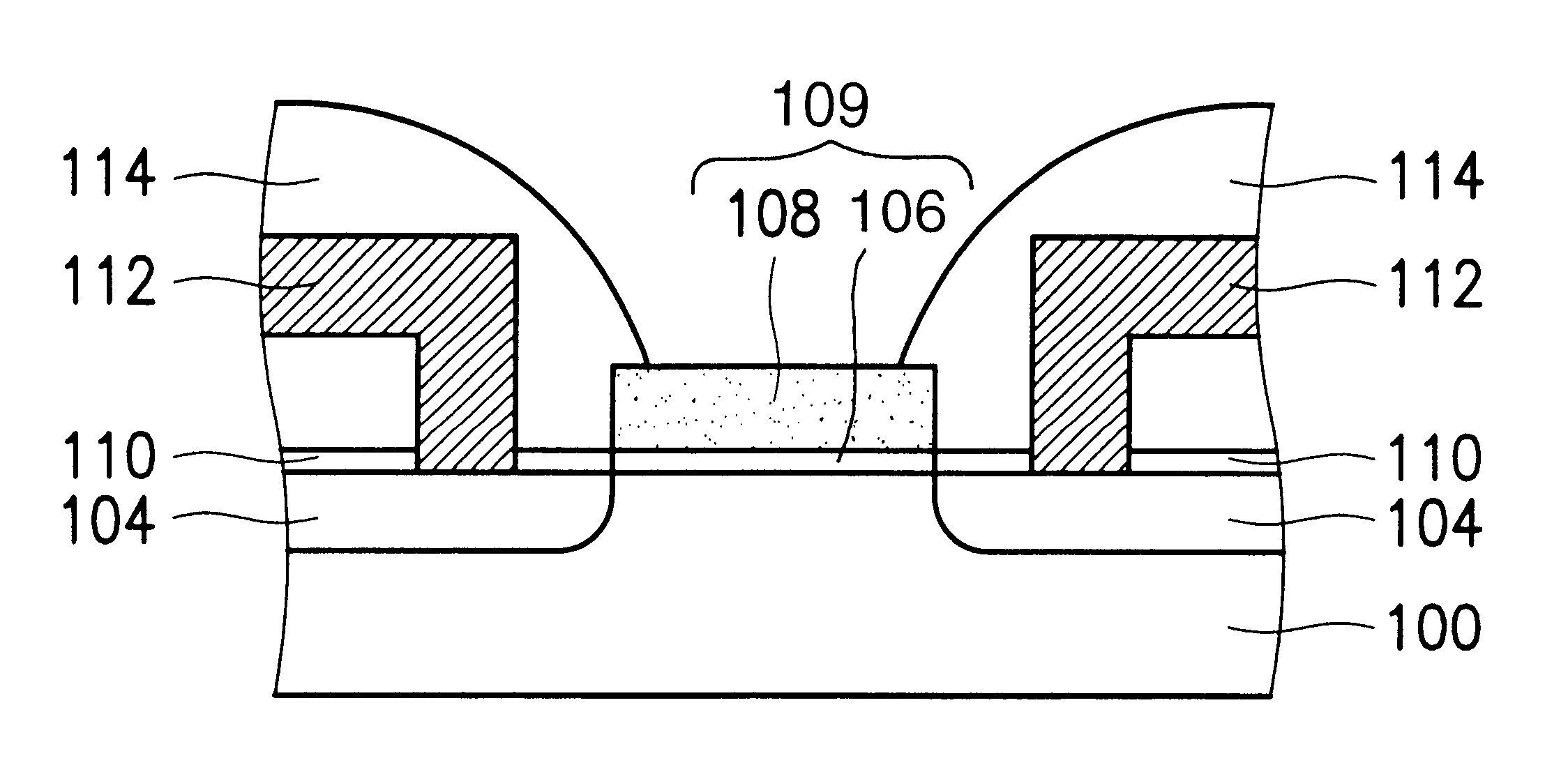
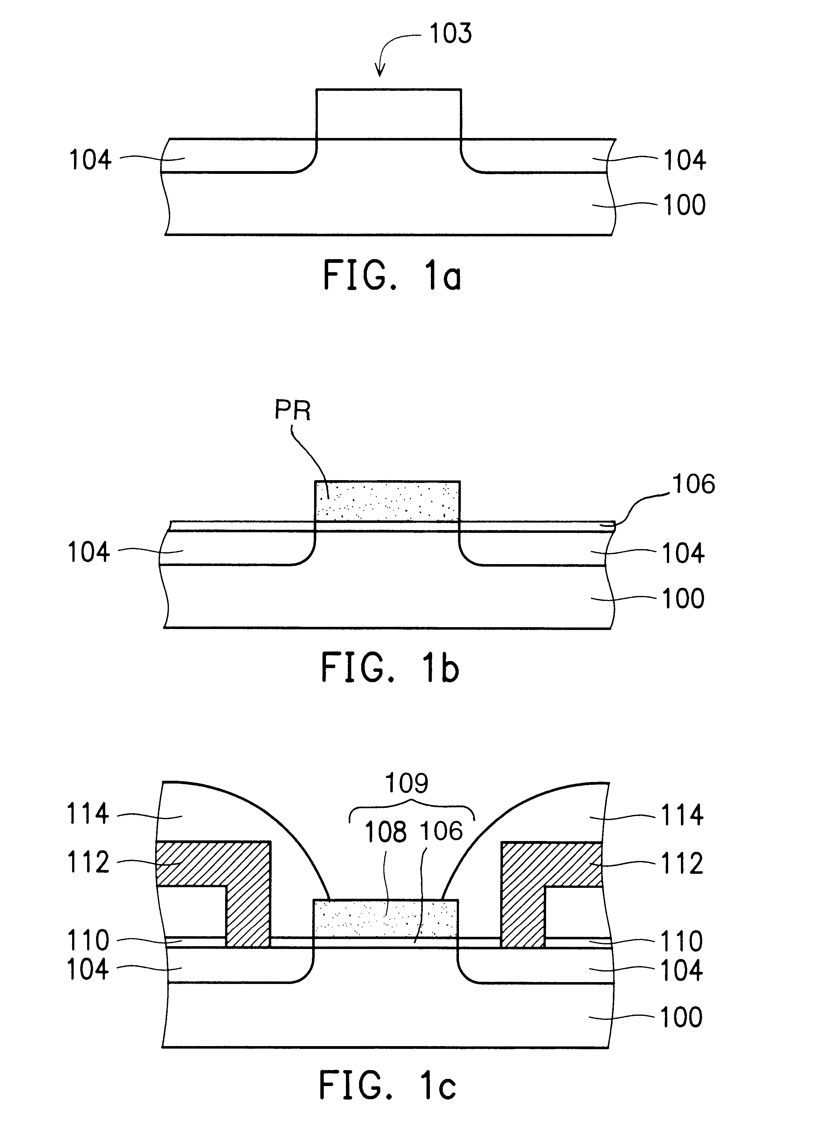
The ion sensitive Field effect transistor (ISFET) according to the embodiment of this invention is illustrated in FIGS. 1a.about.1b.

Referring to FIG. 1a, a P-type (1,0,0) semiconductor substrate 100 with a resistivity ranging from 8 to 12 .OMEGA..multidot.cm was provided. A pad oxide layer consisting of silicon dioxide with a thickness of 5000 .ANG. was formed on the substrate 100 by wet-oxidation. A first photoresist pattern (non-shown) was formed on the pad oxide layer by conventional photolithography. Using the photoresist pattern as a mask, a dummy gate 103 used to define the subsequent gate area was formed by removing a portion of the pad oxide layer.

Then, using the dummy gate 103 as a mask, impurities were implanted into the semiconductor substrate to form a source / drain 104 beside the dummy gate 103. The impurities implanted herein were phosphorous ions with a dose of 10.sup.15 cm.sup.-2.

Referring to FIG. 1b, the dummy gate 103 was removed, that is the pad oxide layer and the...


PUM

PropertyMeasurementUnit
resistivityaaaaaaaaaa
thicknessaaaaaaaaaa
thicknessaaaaaaaaaa

Abstract

Disclosed is an ISFET comprising a H+-sensing membrane consisting of RF-sputtering a-WO3. The a-WO3 / SiO2-gate ISFET of the present invention is very sensitive in aqueous solution, and particularly in acidic aqueous solution. The sensitivity of the present ISFET ranges from 50 to 58 mV / pH. In addition, the disclosed ISFET has high linearity. Accordingly, the disclosed ISFET can be used to detect effluent.

Description

1. Field of the Invention:The invention relates to an ion sensitive field effect transistor (ISFET), and in particular relates to an a-WO.sub.3 -gate ISFET fabricated by RF-sputtering for detecting the hydrogen ions in aqueous solution. In addition, this invention relates to a method for making the a-WO.sub.3 -gate ISFET.2. Description of the Prior Art:The ISFET was first disclosed by P. Bergveld in 1970. The device is a product of applied electrochemistry and microelectronics, and has the function of ion selection and the properties of the FET. This ion sensitive device is strictly different from the traditional ion selection electrode. P. Bergveld disclosed a FET, wherein the metal film set in the gate of traditional FET was removed. Moreover, the device was dipped in electrolyte, wherein no reference electrode was present. However, it was found that a reference electrode must be added to determine the relative voltage between the electrolyte and the semiconductor substrate during...

Claims


Application Information

Patent Timeline
Patent Type & Authority Patents(United States)
IPC IPC(8): G01N27/403G01N27/414
CPCG01N27/414H01L2924/0002H01L2924/00
Inventor CHOU, JUNG CHUANCHIANG, JUNG LUNG
Owner NATIONAL YUNLIN UNIVERSITY OF SCIENCE AND TECHNOLOGY
Why Eureka
Try Eureka