Process for manufacturing a composite polymeric circuit protection device

a protection device and polymer technology, applied in the direction of resistors adapted for applying terminals, positive temperature coefficient thermistors, printed element electric connection formation, etc., can solve the problem of tedious process, and achieve the effect of simple device build-up and inexpensive mass production

Inactive Publication Date: 2003-11-04
LITTELFUSE INC
View PDF141 Cites 30 Cited by
  • Summary
  • Abstract
  • Description
  • Claims
  • Application Information

AI Technical Summary

Benefits of technology

As described in copending, commonly assigned U.S. patent application No. 09/060,278 (Chiang et al, filed Apr. 14, 1998), the disclosure of which is incorporated herein by reference, composite devices can be prepared by sorting individual devices and then assembling the sorted devices into composite devices. Such a process can be tedious, as it may require that the resistance of each individual device be read. We have now found, in accordance with the present invention, that it is possible to prepare a multilayer assembly from which individual composite devices can be divided. Such an assembly allows preparation of a large number of composite devices simultaneously. Furtherm...

Problems solved by technology

Such a process can be tedious, as it may require...

Method used


Image

  • Process for manufacturing a composite polymeric circuit protection device
  • Process for manufacturing a composite polymeric circuit protection device
  • Process for manufacturing a composite polymeric circuit protection device

Examples


example

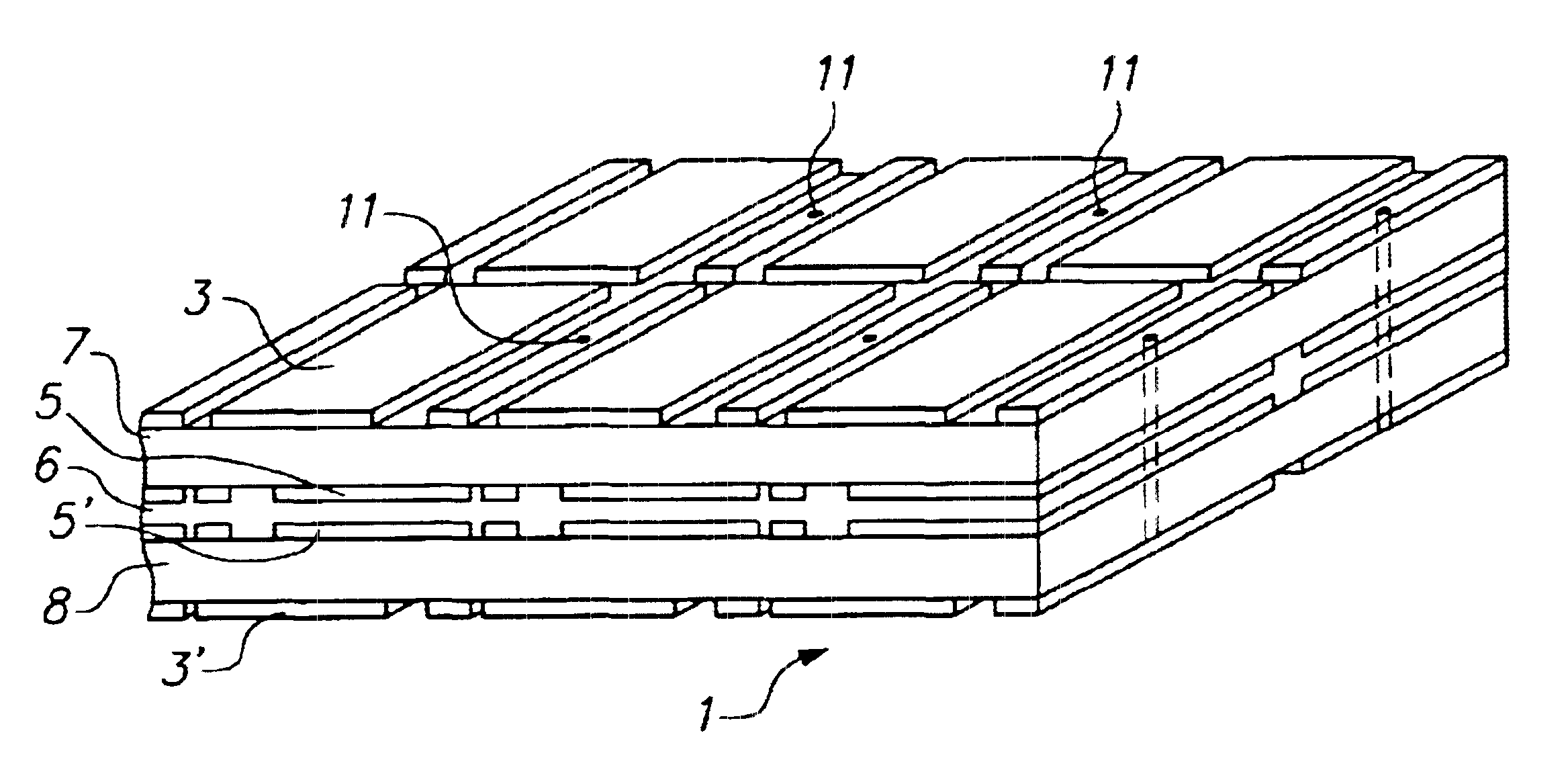
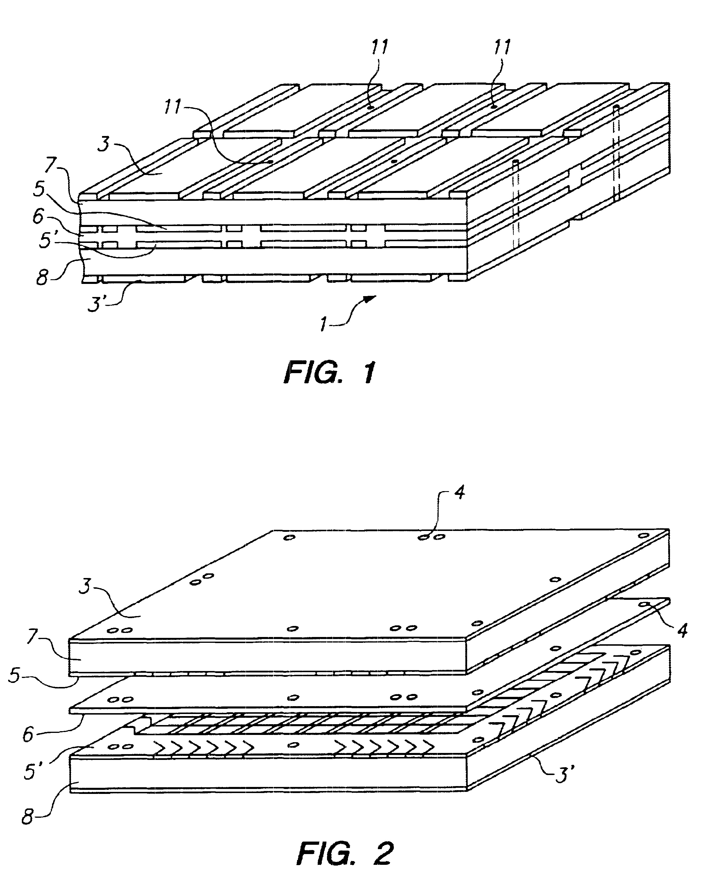
A stack in accordance with FIGS. 1 and 2 was prepared by the following method. Two laminates, each having a thickness of about 0.264 mm (0.0104 inch) were prepared by attaching a nickel / copper foil having a thickness of about 0.0356 mm (0.0014 inch) to both sides of a 0.193 mm (0.0076 inch)-thick sheet of conductive polymer. The conductive polymer was prepared by mixing about 40% by volume carbon black (Raven.TM. 430, available from Columbian Chemicals) with about 60% by volume high density polyethylene (Chevron.TM. 9659, available from Chevron), and then extruding into sheet and laminating in a continuous process. The laminated sheet was cut into individual laminates of 0.30 m.times.0.41 m (12 inch.times.16 inch). The laminates were irradiated to 4.5 Mrad using a 4.5 MeV electron beam.

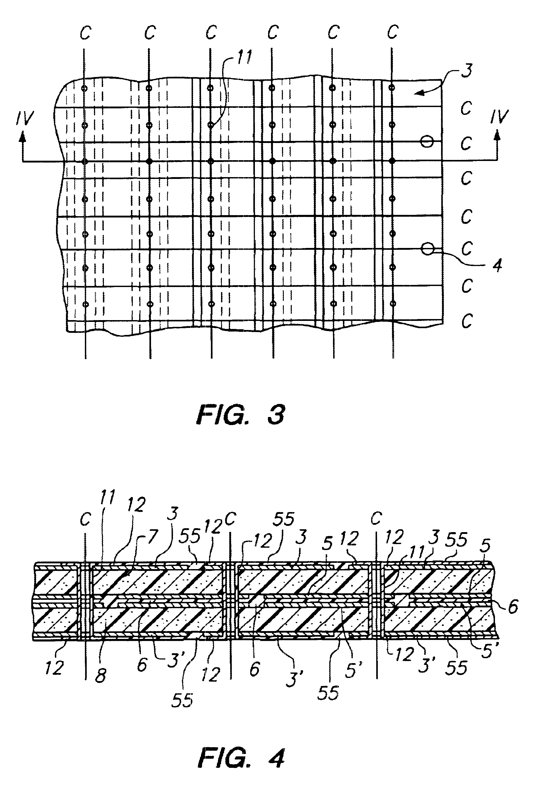
Each of the laminates was drilled in an asymmetric pattern around its the periphery to provide holes and slots to register the laminates in a known x-y orientation in the plane of the laminate. These ...


PUM

PropertyMeasurementUnit
Compositionaaaaaaaaaa
Electrical conductoraaaaaaaaaa
aaaaaaaaaa

Abstract

A process for manufacturing a composite polymeric circuit protection device in which a polymeric assembly is provided and is then subdivided into individual devices. The assembly is made by providing first and second laminates, each of which includes a laminar polymer element having at least one conductive surface, providing a pattern on at least one of the conductive surfaces on one laminate, securing the laminates in a stack in a desired configuration, at least one conductive surface of at least one of the laminates forming an external conductive surface of the stack, and making a plurality of electrical connections between a conductive surface of the first laminate and a conductive surface of the second laminate. The laminar polymer elements may be PTC conductive polymer compositions, so that the individual devices made by the process exhibit PTC behavior.

Description

BACKGROUND OF THE INVENTION1. Field of the InventionThis invention relates to electrical devices and assemblies and methods of making such devices and assemblies.2. Introduction to the InventionCircuit protection devices comprising a conductive polymer composition having a positive temperature coefficient (PTC) are well-known. Such devices which are intended for surface mounting onto a substrate, e.g. a printed circuit board, are disclosed in U.S. Pat. Nos. 5,831,510 (Zhang et al), 5,852,397 (Chan et al), and 5,864,281 (Zhang et al), International Publications Nos. 94 / 01876 (Raychem Corporation) and 95 / 08176 (Raychem Corporation), and copending, commonly assigned application No. 09 / 181,028 (Graves et al, filed Oct. 27, 1998), the disclosures of which are incorporated herein by reference. Such circuit protection devices generally comprise first and second laminar electrodes; a laminar PTC resistive element sandwiched between the electrodes; a third (residual) laminar conductive membe...

Claims


Application Information

Patent Timeline
IPC IPC(8): H01C17/00H01C7/18H01C13/02H01C7/02H01C13/00H01C1/14H05K3/40H05K3/00
CPCH01C1/1406H01C7/027H01C7/18H01C13/02H01C17/006H01C7/021Y10T29/49083H05K3/0052H05K3/403Y10T29/49101Y10T156/1092Y10T29/49085Y10T29/49105Y10T29/49098Y10T29/49082Y10T29/49091Y10T29/49128
Inventor HETHERTON, SCOTTMONTOYA, WAYNEBRUGUIER, THOMASDAERING, RANDY
Owner LITTELFUSE INC
Why Eureka
Try Eureka