Method and system to enhance dynamic range conversion useable with CMOS three-dimensional imaging

Inactive Publication Date: 2004-01-13
MICROSOFT TECH LICENSING LLC
View PDF8 Cites 181 Cited by
  • Summary
  • Abstract
  • Description
  • Claims
  • Application Information

AI Technical Summary

Benefits of technology

In a first embodiment, a low noise, readily replicated circuit promotes a large dynamic range of acquired brightness information. Photodetector output I(t) current is input to a variable gain resettable integrator. The integrator output V(t) is input to a comparator for comparison to a threshold voltage Vth. When V(t).gtoreq.Vth the comparator changes state. A feedback loop from the comparator output to the bias source for the photodetector helps ensure that the comparator output is a time-

Problems solved by technology

During calibration, the phase discriminator forces substantial (but

Method used


Image

  • Method and system to enhance dynamic range conversion useable with CMOS three-dimensional imaging
  • Method and system to enhance dynamic range conversion useable with CMOS three-dimensional imaging
  • Method and system to enhance dynamic range conversion useable with CMOS three-dimensional imaging

Examples


Embodiment Construction

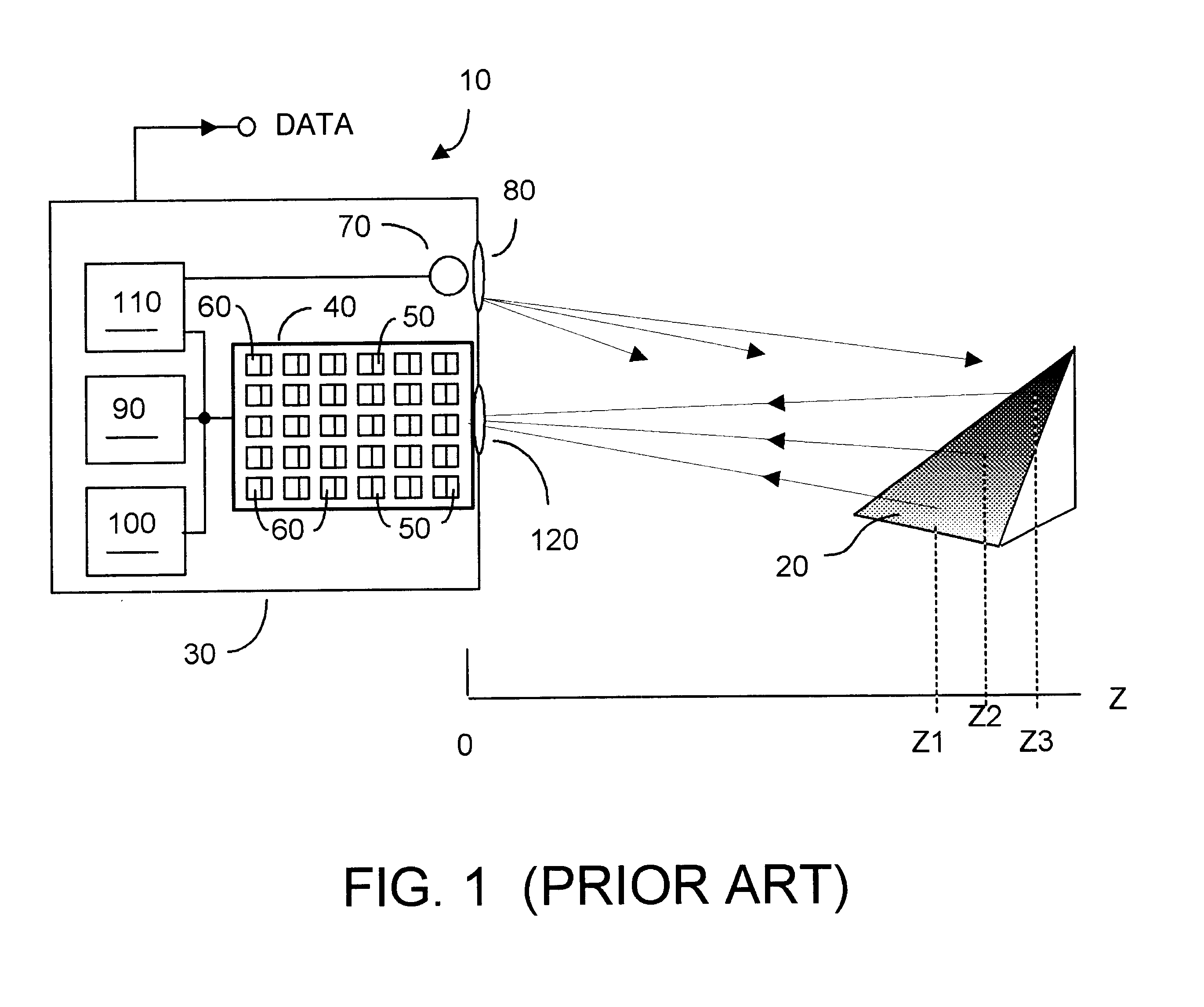
The present invention may be used with a variety of imaging sensing systems, including systems such as that described in U.S. Pat. No. 6,323,942 entitled "CMOS-Compatible Three-Dimensional Image Sensor IC" (2001), assigned to assignee herein. Other systems with which the present invention may be practiced are disclosed in U.S. patent applications Ser. No. 09 / 876,373 entitled "CMOS-Compatible Three-Dimensional Image Sensing Using Reduced Peak Energy", filed Jun. 6, 2001, and Ser. No. 10 / 020,393 entitled "Methods for CMOS-Compatible Three-dimensional Image Sensing Using Quantum Efficiency Modulation", filed Dec. 11, 2001, each application assigned to the assignee herein.

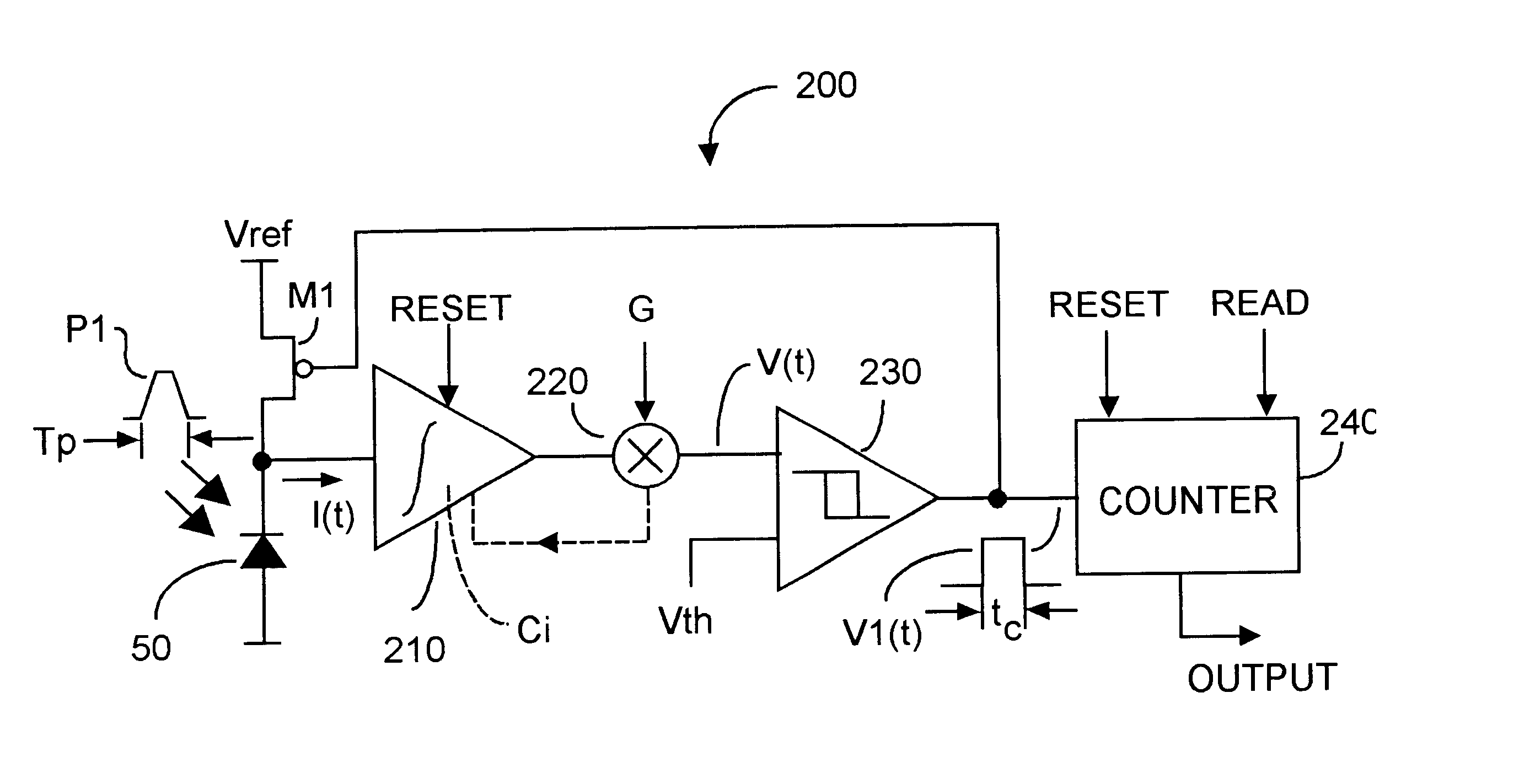
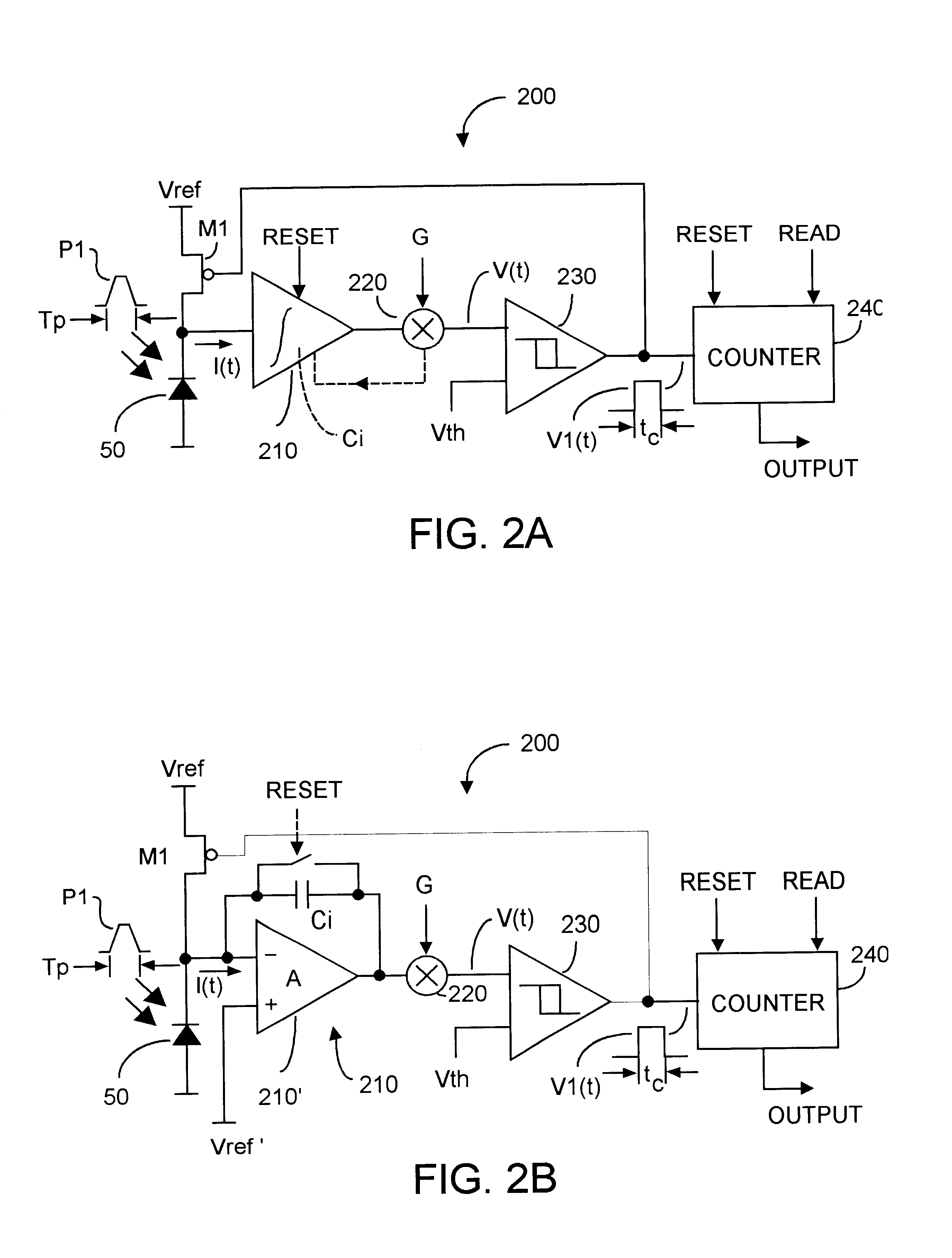
FIG. 2A depicts a generic circuit 200 coupled to a pixel detector or photodiode 50, for example a pixel detector in an array of pixel detectors such as array 40 in FIG. 1. As such, circuit 200 can represent individual circuits 60, shown in FIG. 1. Indeed, circuit 200 may be used with the system of FIG. 1 to improve sys...


PUM


Abstract

High dynamic range brightness information is acquired by inputting detection current to a high (adjustable) gain resettable integrator whose output V(t) is compared to a Vth threshold by a comparator whose output is counted by a reset counter as V(t).gtoreq.Vth. When a desired count is attained, data acquisition ends, the counter is read, and the entire circuit is reset. A TOF data acquisition circuit includes first and second sequences of series-coupled delay units, and a like number of latch units coupled between respective delay units. A phase discriminator compares output from each chain and feedback a signal to one of the chains and to a comparator and can equalize delay through each chain. A control voltage is coupled to the remaining chain to affect through-propagation delay time. The latch units can capture the precise time when V(t).gtoreq.Vth. Successive measurement approximation can enhance TOF resolution.

Description

FIELD OF THE INVENTIONThis invention relates generally to processing data acquired from three-dimensional imaging systems, and more particularly to enhancing the dynamic range associated with data acquired from imaging systems using low-power sequential analog-to-digital conversion, distributed in space and time, including such systems implemented in CMOS.BACKGROUND OF THE INVENTIONImaging sensors are used in a variety of applications, including cameras, video, radar systems, and instrumentation. In generally, such sensors rely upon detection of electromagnetic (EM) energy, for example emitted energy that is reflected off of a target object and then detected.Various techniques are used to detect EM energy, varying upon the application, the energy wavelength, and the desired speed of data acquisition. For example, in radar systems, EM waves are generally focused by a maze of waveguides and detected within a cavity using a diode that is sensitive to the frequency of interest.In light ...

Claims


Application Information

Patent Timeline
IPC IPC(8): H04N3/15H04N5/243H04N5/355H04N5/363H04N5/374
CPCG01S7/487G01S17/08H04N5/243H04N5/363G01S7/4863G01S7/4868G01S17/894H04N23/76H04N25/65
Inventor CHARBON, EDOARDO
Owner MICROSOFT TECH LICENSING LLC
Why Eureka
Try Eureka