Circuit board having improved soldering characteristics

a technology of circuit boards and solder joints, which is applied in the direction of soldering devices, manufacturing tools, coupling device connections, etc., can solve the problems of back pressure building, affecting the flow of solder therein, and preventing the quality of a suitable solder joint from being maintained

Inactive Publication Date: 2004-03-16
DAKTRONICS
View PDF15 Cites 12 Cited by
  • Summary
  • Abstract
  • Description
  • Claims
  • Application Information

AI Technical Summary

Benefits of technology

According to one embodiment of the present invention, there is provided a circuit board having improved soldering characteristics having raised structure consisting of spacer pads arranged to provide for vertical distancing of electrical or electronic components from the component side planar surface of the circuit board to create a vented space between the planar surface of the circuit board and the body of an electronic component as well as a slightly increased size space at the solder station(s). The spacer pads, which can be of different forms, are located in close proximity about the regions where the components are to be located on the component side of the circuit board. One form of a spacer pad can be a stand alone spacer pad and another form can be a spacer pad juxtaposing a solder station, referred to as a terminal spacer pad because of its near location to the solder station or "terminal." Regardless of the form of spacer pad, whether a stand alone spacer pad or a terminal spacer pad, the upper surface of each spacer pad projects a like distance above the planar surface of the circuit board to provide for component spacing from the planar surface of the circuit board. More importantly, such spacer pads raise the lower surface of the component above the levels of the solder stations so that venting is allowed and provided extending upwardly through the circuit board at the upper region of the circuit board at the solder stations. Such venting allows for escaping of gases through the upper regions of the solder stations to negate a vapor lock, thus allowing unimpeded flow of molten solder therein in a timely fashion to effect a proper solder joint.
One significant aspect and feature of the present invention is a circuit board having improved soldering characteristics.
Still another significant aspect and feature of the present invention is the use of spacer pads to provide a clear area at the upper region of the solder station for the clear passage release and unrestricted flow of gases upwardly during the soldering process, thus allowing solder flow unimpeded therein to effect a proper solder joint.
Yet another significant aspect and feature of the present invention is the spacing of components above the circuit board to increase cooling airflow around the undersides of the components.
Having thus described embodiments of the present invention, it is the principal object of the present invention to provide a circuit board having improved soldering characteristics.

Problems solved by technology

Maintaining the quality of a suitable solder joint can be problematic in that a cold solder joint may be produced when solder cannot flow fully into the region of intended solder flow.
Such a problem can be caused due to limited or non-existent gas flow and breathing within or above the region of intended solder flow, such as caused by the region of intended solder flow being a closed space having a pneumatic-like seal whereby solder flow cannot reach the region of intended solder flow, or if the solder does reach the region of intended solder flow, the heat is dissipated due to slow movement of the solder before sufficient heating of the solder joint takes place.
Additionally, air or other gases trapped in the upper region of intended solder flow cannot be displaced by the solder flow, and a back pressure may build to impede the flow of solder therein.

Method used


Image

  • Circuit board having improved soldering characteristics
  • Circuit board having improved soldering characteristics
  • Circuit board having improved soldering characteristics

Examples


Embodiment Construction

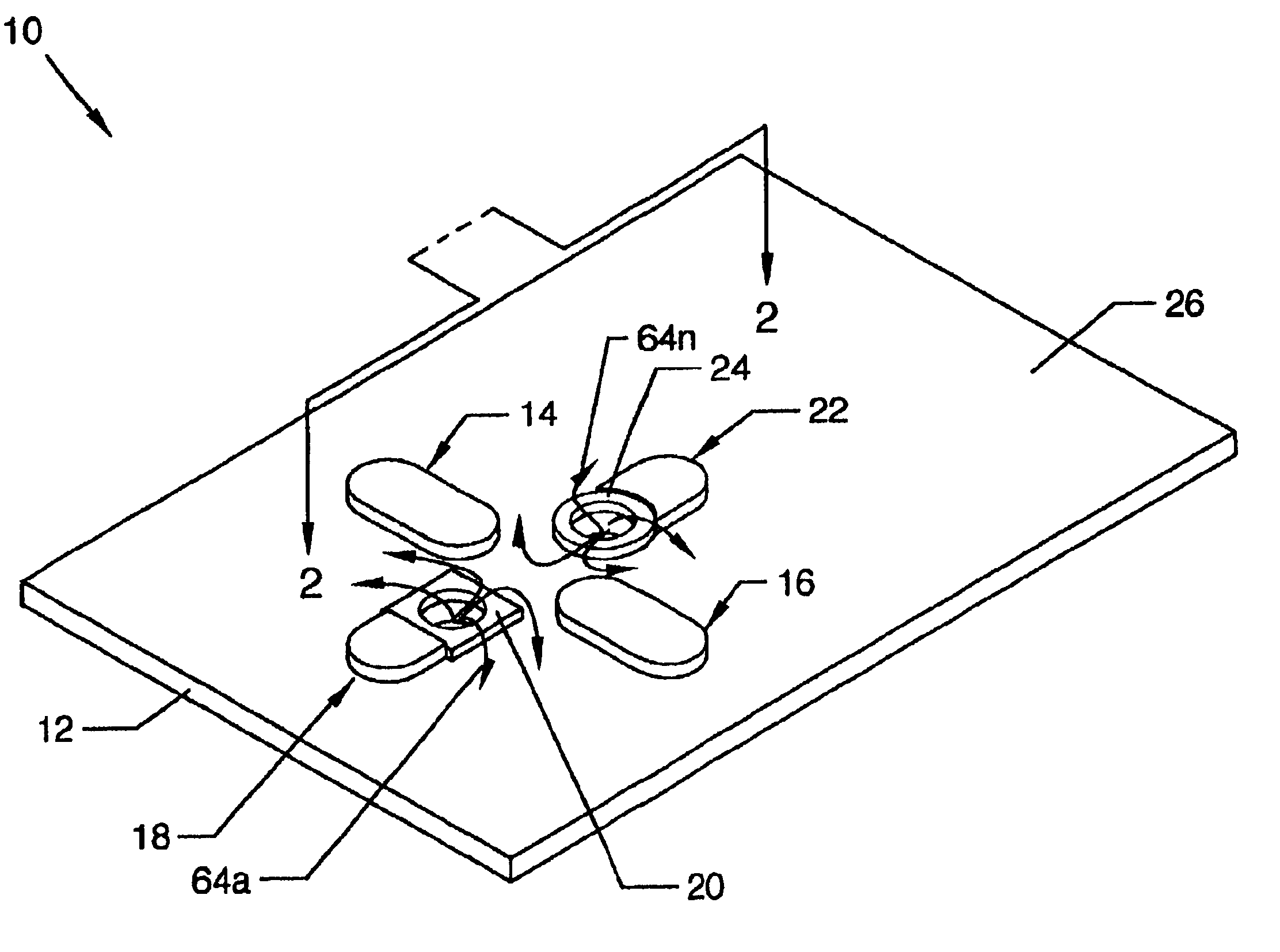
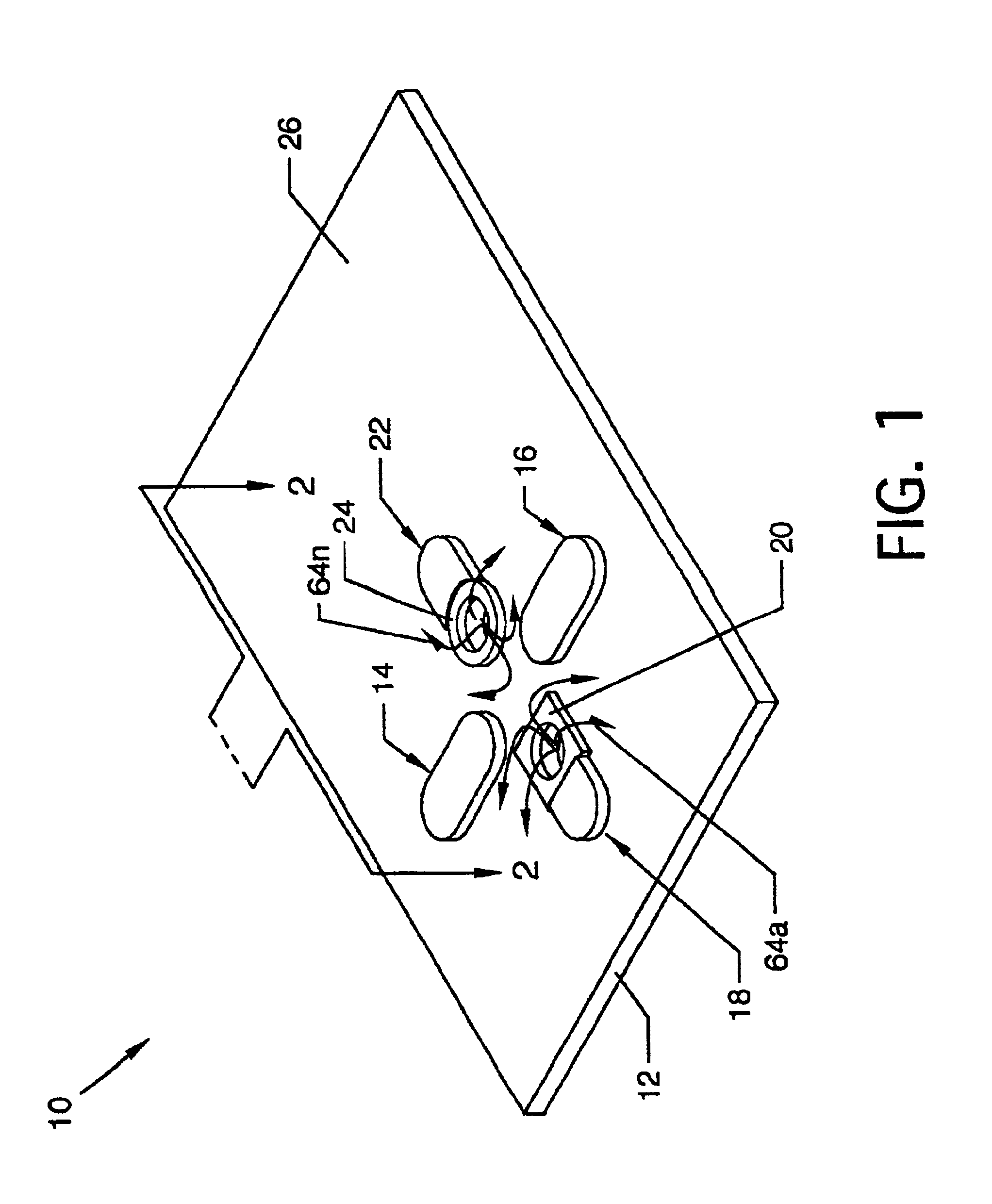
FIG. 4 illustrates a close cross sectional view of FIG. 3 along line 4--4 of FIG. 3. Solder 60 is applied by wave soldering techniques to flow liquidized solder into solder stations such as solder station 20. Gases 62 given off by the soldering process rise vertically and unimpeded through the passage 56 and then travel horizontally and unimpeded along the space 55 which connects to the passage 56 and thence along the bottom surface 52 of the LED 50 and then outwardly to atmosphere, as shown in the illustration. Such paths of gaseous flow are shown by arrows 64a-64n in FIG. 1 where the gaseous flow rises vertically and then horizontally through and about and along the solder stations 20 and 24 and beneath the spaced electronic component (not shown) and thence to atmosphere.

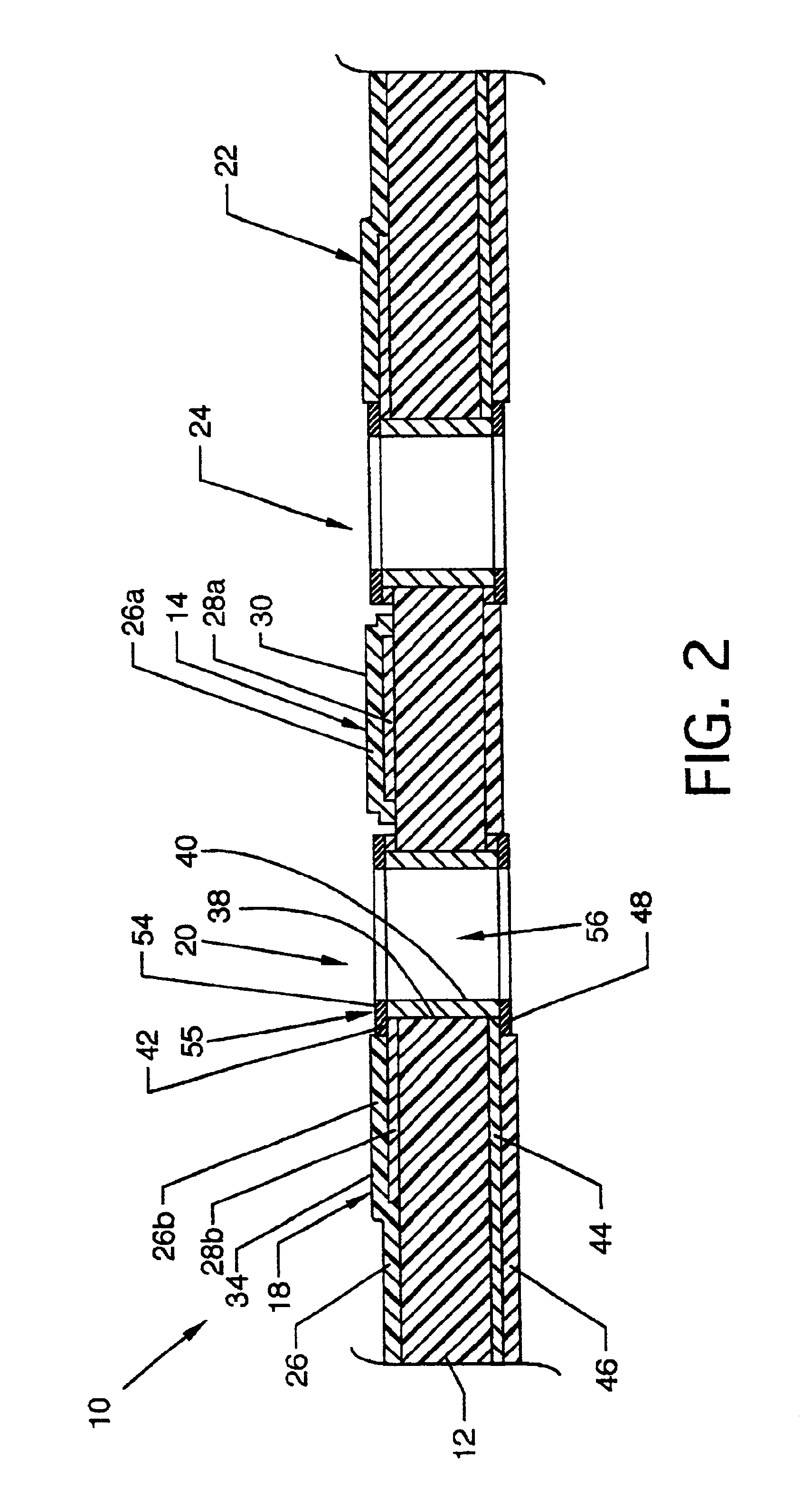
FIG. 5, an alternate embodiment, illustrates a cross section view of a circuit board having improved soldering characteristics 10a, including much of the structure of the previously described embodiment, having mo...


PUM

PropertyMeasurementUnit
electrically conductiveaaaaaaaaaa
perimeteraaaaaaaaaa
distanceaaaaaaaaaa

Abstract

A circuit board having improved soldering characteristics having raised structure consisting of spacer pads arranged to provide for vertical distancing of electrical or electronic components from the component side planar surface of the circuit board. Such spacing is complementary to top vented soldering stations where the spacing allows solder process gases to flow unimpeded from the soldering stations through the spacing to atmosphere.

Description

None.1. Field of the InventionThe present invention is for a circuit board, and more particularly, is for a circuit board having improved soldering characteristics with respect to components which can be secured to a circuit board such as by soldering.2. Description of the Prior ArtPrior art circuit boards often utilize wave soldering techniques to flow liquidized solder at a raised temperature along one surface or more of a circuit board to effect multiple solder joints between the soldering pads of the circuit board and the leads of one or more electrical or electronic components such as, but not limited to, a light emitting diode. Maintaining the quality of a suitable solder joint can be problematic in that a cold solder joint may be produced when solder cannot flow fully into the region of intended solder flow. Such a problem can be caused due to limited or non-existent gas flow and breathing within or above the region of intended solder flow, such as caused by the region of int...

Claims


Application Information

Patent Timeline
Patent Type & Authority Patents(United States)
IPC IPC(8): H05K3/34H05K3/30
CPCH05K3/306H05K3/3447H05K3/3452H05K2201/09781H05K2201/099H05K2201/10106H05K2201/10651H05K2201/2036H05K2203/1178
Inventor BRAVEK, ERIC S.UEHRAN, RANDY S.
Owner DAKTRONICS
Why Eureka
Try Eureka