Apparatus for attaching resists and wafers to substrates
a technology for attaching apparatuses and resists, which is applied in the direction of soldering apparatus, manufacturing tools,auxillary welding devices, etc., can solve the problems that the automatic attachment process of resists cannot only save enormous labor costs, reduce process costs, and improve process efficiency, so as to save enormous labor costs and improve process costs. , the effect of improving efficiency
- Summary
- Abstract
- Description
- Claims
- Application Information
AI Technical Summary
Benefits of technology
Problems solved by technology
Method used
Image

Examples
Embodiment Construction
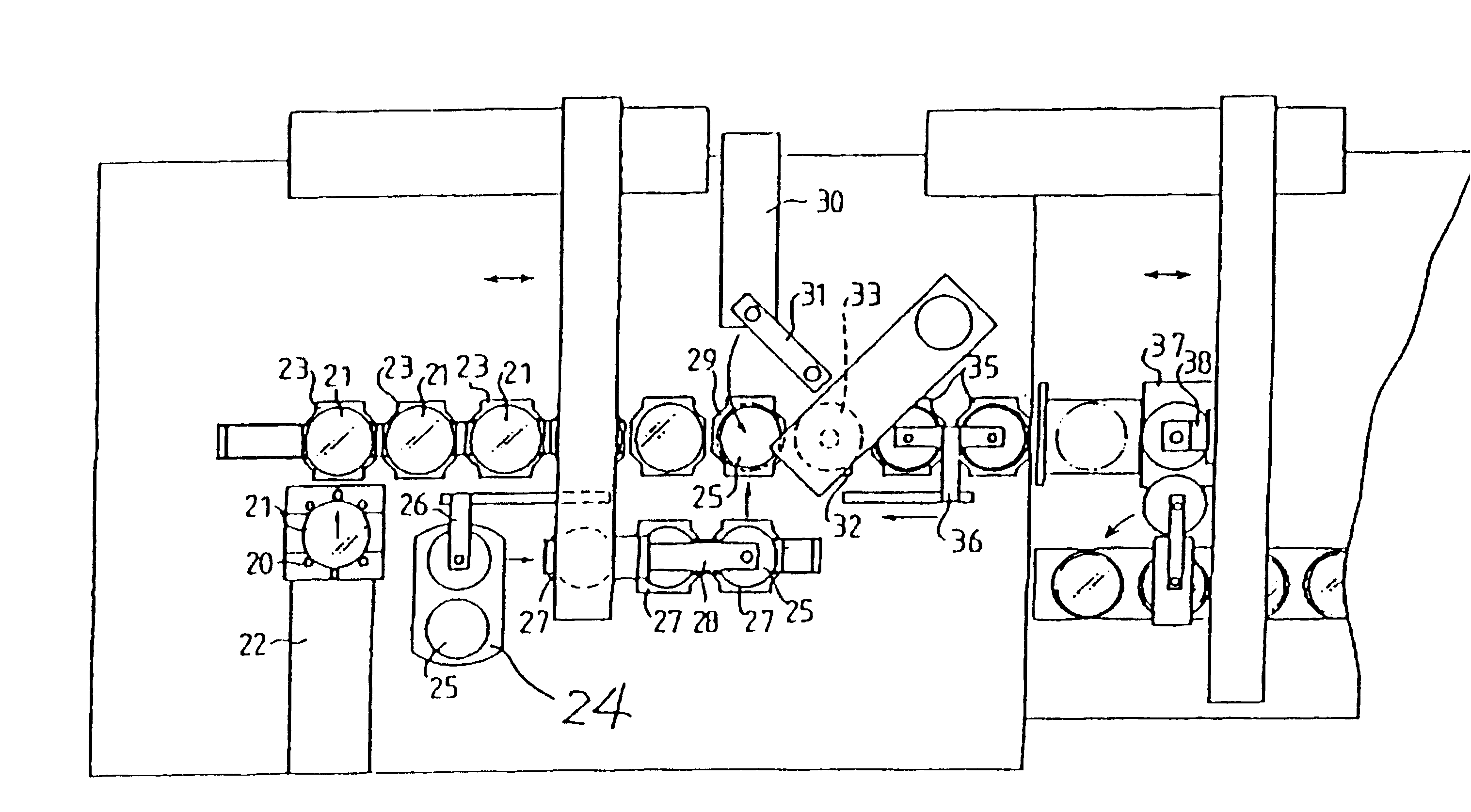
This invention is related to an apparatus for attaching resists and wafers to substrates which is mainly utilized in the process of manufacturing semiconductors. The detailed steps provided by the apparatus of the preferred embodiment of this invention are shown in the flow chart of FIG. 4, and the construction of the apparatus of the preferred embodiment is illustrated in FIGS. 5 to 8. According to this invention, the apparatus for attaching resists and wafers to substrates comprises a first magazine 20, as shown in FIGS. 5 and 6, for holding a plurality of substrates. In the preferred embodiment of this invention, the substrates are glass plates 21 being stacked piece by piece within the first magazine 20 (step 400). The glass plate 21 is pushed to a first hot plate 23 for preheating by a first moving device 22 (step 401). The apparatus of this invention also has a second magazine 24 for holding a plurality of wafers 25 which are stacked piece by piece therein (step 410). The wafe...
PUM
| Property | Measurement | Unit |
|---|---|---|
| Angle | aaaaa | aaaaa |
| Temperature | aaaaa | aaaaa |
| Thickness | aaaaa | aaaaa |
Abstract
Description
Claims
Application Information