Ferroelectric memory and electronic apparatus

a technology of electronic equipment and ferroelectric memory, which is applied in the direction of transistors, solid-state devices, instruments, etc., can solve the problems of difficult to be oriented in the direction of "a" axis, the angularity of hysteresis curve becomes inferior, and the type of ferroelectric memory cannot be realized

Inactive Publication Date: 2004-04-13
SEIKO EPSON CORP
View PDF6 Cites 5 Cited by
  • Summary
  • Abstract
  • Description
  • Claims
  • Application Information

AI Technical Summary

Benefits of technology

According to the above structure, epitaxaial growth of SrBi.sub.2 Ta.sub.2 O.sub.9 ferroelectric layer is possible on a Si single crystal substrate, and an effect that ferroelectric memory having superior angularity in hysteresis curve is obtained.
According to the above structure, the ferroelectric memory has compatibility of memory characteristics and integrity; therefore, reliable and small electronic apparatus can be obtained.

Problems solved by technology

Although an MFSFET type is advantageous in terms of high integration and non-destructive readout, this type ferroelectric memory has not be realized yet due to the structural difficulty in manufacturing; therefore, the capacitor type ferroelectric memory antecedes the MFSFET type in developing and launching into market presently.
However, when a ferroelectric capacitor is constructed using SBT as a Ferroelectric, there were following problems.
But, SBT has a layered structure; even though it is easy to be oriented in direction of "c" axis, it is very difficult to be oriented in direction of "a" axis.
Also, in a non-oriented polycrystal layer, an angle between the polarization axis of each crystal grain and the charged electric field is not uniform; thus, the charged voltage when a domain inversion occur in each crystal grain is not uniform, and the angularity of hysteresis curve becomes inferior.

Method used


Image

  • Ferroelectric memory and electronic apparatus
  • Ferroelectric memory and electronic apparatus
  • Ferroelectric memory and electronic apparatus

Examples


first embodiment

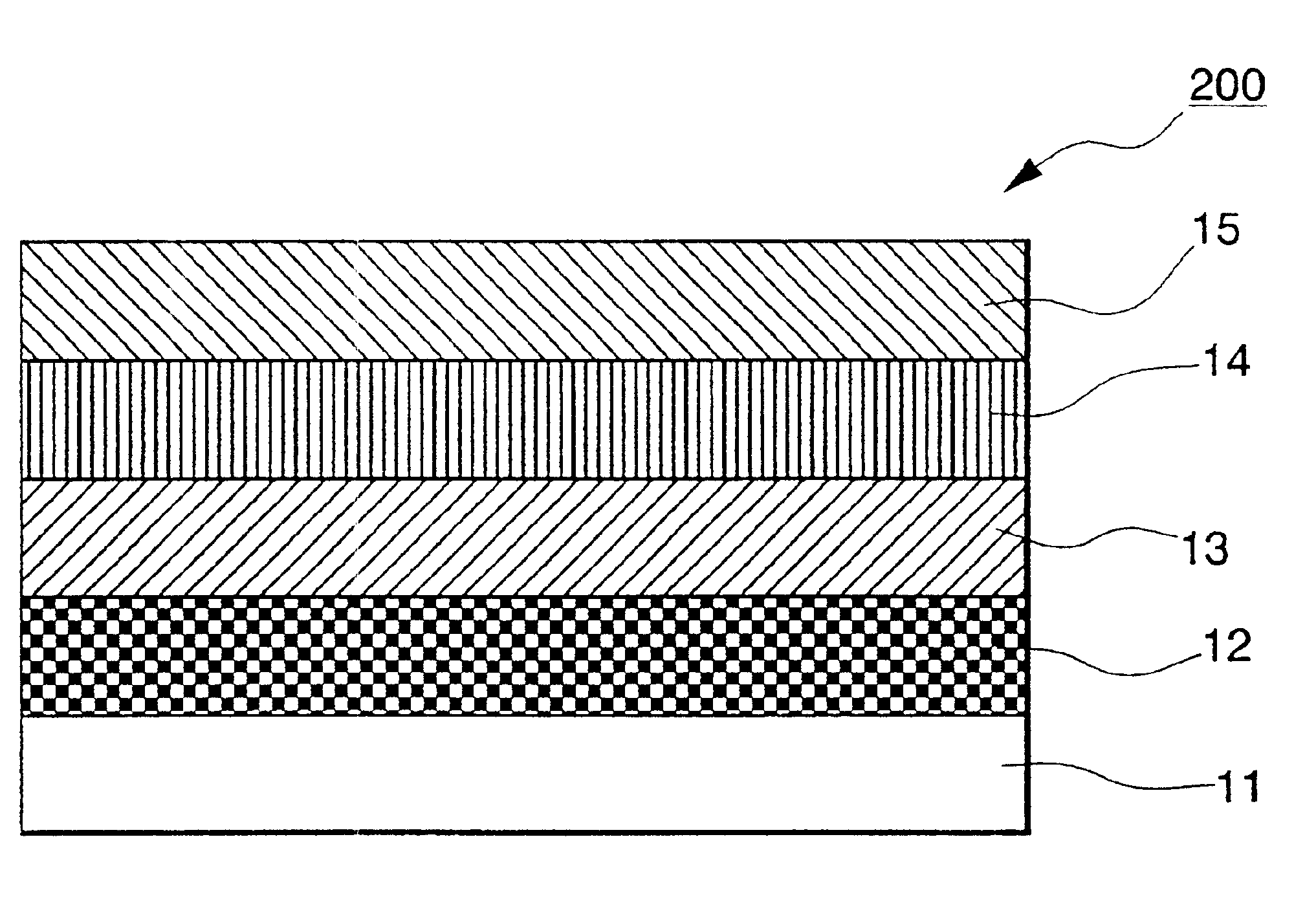
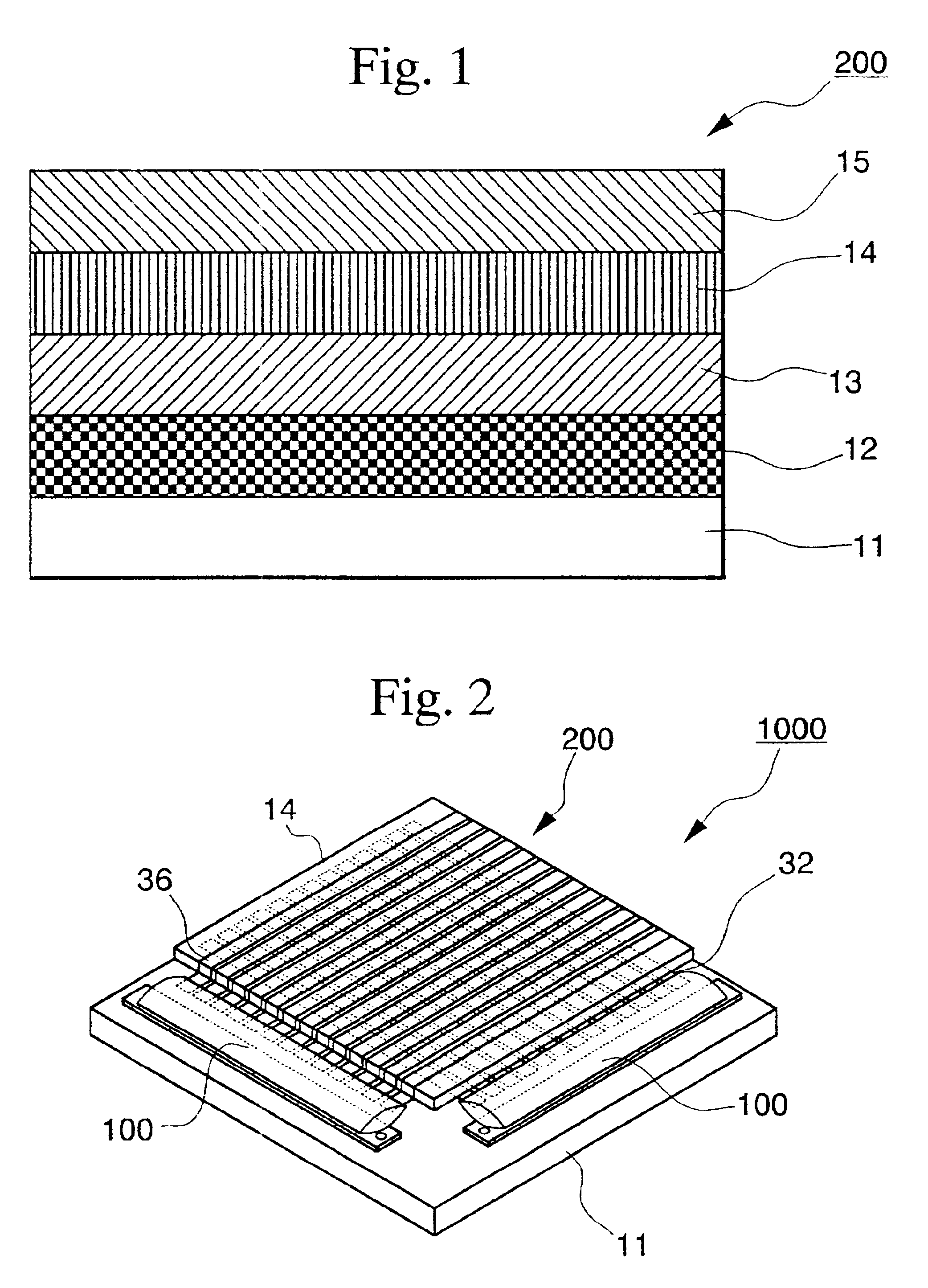
FIG. 1 is a cross section showing the first embodiment of a ferroelectric memory (memory cell).

5 nm of buffer layer 12 composed of YSZ having fluorite structure was layered on a (100) Si single crystal substrate 11 under condition that the temperature of the substrate is 700 degrees Celsius and partial pressure of oxygen is 1.times.10.sup.-5 Torr with laser abrasion method using yttrium stabilized zirconia YSZ target. The temperature of the substrate and the partial pressure of oxygen are not limited above conditions.

Next, 100 nm of SrRuO.sub.3 bottom electrode layer 13 having perovskite structure was layered on a buffer layer 12 composed of YSZ under condition that the temperature of the substrate is 700 degrees Celsius and partial pressure of oxygen is 1.times.10.sup.-2 Torr with laser abrasion method using SrRuO.sub.3 target. The temperature of the substrate and the partial pressure of oxygen are not limited above conditions.

Furthermore, 100 nm of SrBi.sub.2 Ta.sub.2 O.sub.9 ferr...

second embodiment

FIG. 1 is a cross section showing the second embodiment of the ferroelectric memory of the present invention, therefore FIG. 1 shows the same structure as is shown in the first embodiment. However, the direction of disposition of the layer and the substrate, and the material are different from the case of the first embodiment.

5 nm of buffer layer 12 composed of SrO having NaCl structure was layered on a (110) Si single crystal substrate 11 under condition that the temperature of the substrate is 700 degrees Celsius and partial pressure of oxygen is 1.times.10.sup.-6 Torr with laser abrasion method using SrO.sub.2 target. The temperature of the substrate and the partial pressure of oxygen are not limited above conditions.

Next, 100 nm of SrRuO.sub.3 bottom electrode layer 13 having perovskite structure was layered on a buffer layer 12 composed of SrO under condition that the temperature of the substrate is 700 degrees Celsius and partial pressure of oxygen is 1.times.10.sup.-2 Torr wi...

third embodiment

FIG. 1 is a cross section showing the third embodiment of the ferroelectric memory of the present invention, therefore FIG. 1 shows the same structures as is shown in the first and the second embodiments. However, the direction of disposition of the layer and the substrate, and the material are different from the case of the first and the second embodiment.

5 nm of buffer layer 12 composed of SrO having NaCl structure was layered on a (111) Si single crystal substrate 11 under condition that the temperature of the substrate is 700 degrees Celsius and partial pressure of oxygen is 1.times.10.sup.-6 Torr with laser abrasion method using SrO.sub.2 target. The temperature of the substrate and the partial pressure of oxygen are not limited above conditions.

Next, 100 nm of SrRuO.sub.3 bottom electrode layer 13 having perovskite structure was layered on a buffer layer 12 composed of SrO under condition that the temperature of the substrate is 700 degrees Celsius and partial pressure of oxyg...


PUM

PropertyMeasurementUnit
temperatureaaaaaaaaaa
coercive electric fieldaaaaaaaaaa
ferroelectricaaaaaaaaaa

Abstract

In case capacitor-type ferroelectric memory is formed by using SrB2Ta2O9 having superior fatigue resistance for ferroelectric layer, non-orientation layer is inferior in angularity, and SBT of orientation layer is subject to be oriented to c-axis orientation, polarization moment of a-axis direction was not effectively used, on Si single crystal substrate, a buffer layer and a bottom electrode layer composed of conductive oxide having perovskite structure are grown in epitaxially, furthermore the epitaxial growth of ferroelectric layer composed of SBT is performed with slanting c-axis to the substrate by 45 to 55 degrees.

Description

1. Field of the InventionThe present invention relates to a ferroeletric memory using metal oxide layer and an electronic apparatus using the ferroelectric memory.2. Description of Related ArtFerroelectric memory has udergone rapid development in recent years as a form of nonvolatile memory employing a ferroelectric substance. A ferroelectric memory can be categorized into a capacitor type forming a 1T / 1C structure or the like if a Ferroelectric is used as a capacitor and an MFSFET in which Ferroelectric is used type as a gate insulator for a field effect transistor instead of SiO.sub.2. Although an MFSFET type is advantageous in terms of high integration and non-destructive readout, this type ferroelectric memory has not be realized yet due to the structural difficulty in manufacturing; therefore, the capacitor type ferroelectric memory antecedes the MFSFET type in developing and launching into market presently.The material for Ferroelectric used for the capacitor type ferroelectri...

Claims


Application Information

Patent Timeline
Patent Type & Authority Patents(United States)
IPC IPC(8): G11C11/22H01L27/105H01L21/8246
CPCG11C11/22
Inventor HIGUCHI, TAKAMITSUIWASHITA, SETSUYAMIYAZAWA, HIROMU
Owner SEIKO EPSON CORP
Why Eureka
Try Eureka