Methods of driving an array of optical elements

an array and optical element technology, applied in the field of methods of driving arrays of optical elements, can solve the problems of image sticking, slow operation of cells, and a short life, and achieve the effects of avoiding image sticking, avoiding image sticking, and avoiding image sticking

Inactive Publication Date: 2004-07-13
QINETIQ LTD
View PDF7 Cites 107 Cited by
  • Summary
  • Abstract
  • Description
  • Claims
  • Application Information

AI Technical Summary

Benefits of technology

It is desirable that between the first and second steps all the elements of the array are simultaneously addressed to impose zero potential difference thereacross. This serves effectively to provide a defined period for each individual element during which dc has been applied across it, and so enables dc balance to be more precisely determined.

Problems solved by technology

Such cells were slow to operate and tended to have a short life due to degradation of the liquid crystal material.
When driving liquid crystal electro-optic devices for any length of time, a phenomenon known as image sticking may occur.
Furthermore, the switching time from a wholly "OFF" state to a wholly "ON" state tends to be rather long, commonly around a millisecond.
While the latter arrangements provided considerable versatility, there were problems associated with cross-talk between pixels.
Addressing schemes became relatively complicated, particularly if dc balance was also required.
Such considerations, in association with the relative slowness of switching of nematic cells, have made is difficult to provide real-time video images having a reasonable resolution.
This can lead to problems, especially with DRAM type backplanes where the pixels are part of the DRAM circuit, including photo-induced conductivity and charge leakage.
Nevertheless, there are problems associated with the yields of the backplanes during manufacture, and the length of the addressing conductors has a slowing effect on the scanning.
Semiconductor active backplanes are limited in size to the size of semiconductor substrate available, and are not suited for direct viewing with no intervening optics.
However, as the liquid crystal thickness approaches the thicknesses associated with the underlying structure of the backplane, and any possible deformation of the liquid crystal cell structure by flexing or other movement of the substrates, problems arise, for example as to the uniformity of response across the pixel area, and the capability for short circuiting across the cell thickness.
If the addressing pulse is insufficiently long for transfer of the requisite amount of charge, the capacitive element is incompletely switched.
However, in order to apply appropriate electric fields for switching, very small electrode gaps are required and therefore such devices tend to have very small active areas, and as a consequence this type of device is relatively uncommon.
In practice, it is very difficult or impossible to obtain true bistability, especially on silicon backplanes and there will a slight preference for one state over the other.
Nevertheless, this should give rise to relatively long relaxation times.
Therefore, if a switched pixel is completely electrically isolated, charge cannot flow and the pixel cannot relax.
In practice, charge leakage cannot be completely eliminated, and so relaxation will occur, but over an extended period.
A common cause of charge leakage is photoconductivity associated with the slug capacitance mentioned earlier and / or photoconductive or other leakage currents in the associated switching transistor of the DRAM array.
However, modern computing methods and standards converters have tended to make other formats redundant in the majority of cases.

Method used


Image

  • Methods of driving an array of optical elements
  • Methods of driving an array of optical elements
  • Methods of driving an array of optical elements

Examples


Embodiment Construction

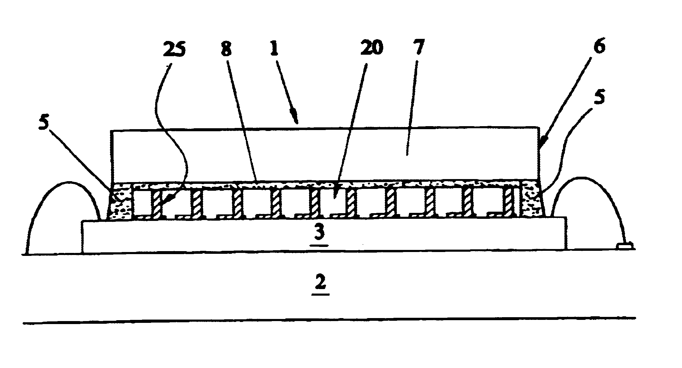
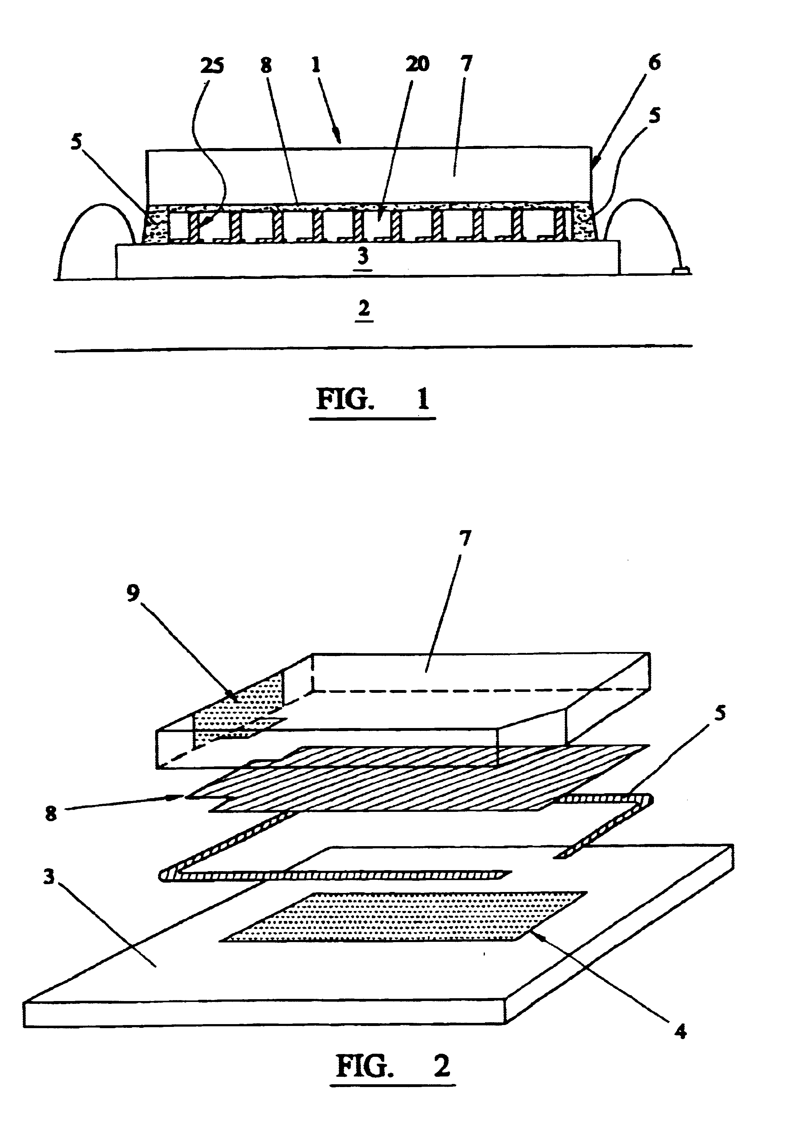
FIG. 1 shows in schematic cross-sectional view a liquid crystal cell 1 mounted on a thick film alumina hybrid substrate or chip carrier 2. The cell 1 is shown in exploded view in FIG. 2. The use of a hybrid substrate for mounting electro-optic devices is discussed in more detail in our copending application PCT / GB99 / 04285, ref: P20957WO.

Cell 1 comprises an active silicon backplane 3 in which a central region is formed to provide an array 4 of active mirror pixel elements arranged in 320 columns and 240 rows. Outside the array, but spaced from the edges of the backplane 3, is a peripheral glue seal 5, which seals the backplane 3 to the peripheral region of a front electrode 6. FIG. 2 shows that the glue seal is broken to permit insertion of the liquid crystal material into the assembled cell, after which the seal is completed, either by more of the same glue, or by any other suitable material or means known per se.

Front electrode 6 comprises a generally rectangular planar glass or si...


PUM

PropertyMeasurementUnit
thicknessaaaaaaaaaa
cone angleaaaaaaaaaa

Abstract

Relates to writing an array of optical elements which are each switched between two states according to input data sets. In a first method, data is written in two steps in which different selected elements are respectively driven to one binary state and the other binary state. The selected elements of the two sets may be complementary, but are preferably only those which are required to change from their existing state. The latter criterion may be used in an alternative method using a single addressing of the array to turn elements in either direction as required. In a further method, as shown, selected elements only of a blank array are written in a first WRITE step so as to correspond with a set of data, and in a subsequent second ERASE step the selected elements are selectively erased to restore a blank array prior to writing and erasing another set of data. The methods have particular utility for maintaining a dc balance at pixels of a liquid crystal array.

Description

This application in the U.S. national phase of International Application No. PCT / GB99 / 04275, filed Dec. 16, 1999, the entire content of which is hereby incorporated by reference.1. Field of the InventionThe present invention relates to methods of driving a array of optical elements. It has particular but not exclusive relevance to the driving of a spatial light modulator.2. Discussion of Prior ArtThe spatial light modulator to be described in relation to a preferred embodiment in this specification is a in the form of a smectic liquid crystal layer disposed between an active semiconductor backplane and a common front electrode. It was developed in response to a requirement for a fast and, if possible, inexpensive, spatial light modulator comprising a relatively large number of pixels with potential application not only as a display device, but also for other forms of optical processing such as correlation and holographic switching. Other aspects of this device are dealt with in our ...

Claims


Application Information

Patent Timeline
Patent Type & Authority Patents(United States)
IPC IPC(8): G09G3/36G09G3/20G02F1/133
CPCG09G3/3651G09G3/2018G09G3/3655G09G3/3674G09G3/3685G09G2310/0245G09G2310/0297G09G2310/04G09G2310/06G09G2320/0606G09G2320/0626
Inventor COKER, TIMOTHY MCROSSLAND, WILLIAM A
Owner QINETIQ LTD
Why Eureka
Try Eureka